China Wafer Manufacturers, Suppliers, Factory
What is the semiconductor wafer?
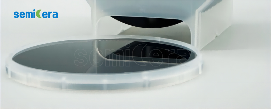
A semiconductor wafer is a thin, round slice of semiconductor material that serves as the foundation for the fabrication of integrated circuits (ICs) and other electronic devices. The wafer provides a flat and uniform surface on which various electronic components are built.
The wafer manufacturing process involves several steps, including growing a large single crystal of the desired semiconductor material, slicing the crystal into thin wafers using a diamond saw, and then polishing and cleaning the wafers to remove any surface defects or impurities. The resulting wafers have a highly flat and smooth surface, which is crucial for the subsequent fabrication processes.
Once the wafers are prepared, they undergo a series of semiconductor manufacturing processes, such as photolithography, etching, deposition, and doping, to create the intricate patterns and layers required to build electronic components. These processes are repeated multiple times on a single wafer to create multiple integrated circuits or other devices.
After the fabrication process is complete, the individual chips are separated by dicing the wafer along predefined lines. The separated chips are then packaged to protect them and provide electrical connections for integration into electronic devices.
Different materials on wafer
Semiconductor wafers are primarily made from single-crystal silicon due to its abundance, excellent electrical properties, and compatibility with standard semiconductor manufacturing processes. However, depending on specific applications and requirements, other materials can also be used to make wafers. Here are some examples:
Silicon carbide (SiC) is a wide bandgap semiconductor material that offers superior physical properties compared to traditional materials. It helps reduce the size and weight of discrete devices, modules, and even entire systems, while improving efficiency.
Key Characteristics of SiC:
- -Wide Bandgap: SiC's bandgap is about three times that of silicon, allowing it to operate at higher temperatures, up to 400°C.
- -High Critical Breakdown Field: SiC can withstand up to ten times the electric field of silicon, making it ideal for high-voltage devices.
- -High Thermal Conductivity: SiC efficiently dissipates heat, helping devices maintain optimal operating temperatures and prolonging their lifespan.
- -High Saturation Electron Drift Velocity: With double the drift velocity of silicon, SiC enables higher switching frequencies, aiding in device miniaturization.
Applications:
-
-Power Electronics: SiC power devices excel in high-voltage, high-current, high-temperature, and high-frequency environments, significantly enhancing energy conversion efficiency. They are widely used in electric vehicles, charging stations, photovoltaic systems, rail transportation, and smart grids.
-
-Microwave Communications: SiC-based GaN RF devices are crucial for wireless communication infrastructure, especially for 5G base stations. These devices combine SiC's excellent thermal conductivity with GaN's high-frequency, high-power RF output, making them the preferred choice for next-generation high-frequency telecom networks.
Gallium nitride (GaN) is a third-generation wide bandgap semiconductor material with a large bandgap, high thermal conductivity, high electron saturation drift velocity, and excellent breakdown field characteristics. GaN devices have broad application prospects in high-frequency, high-speed, and high-power areas such as LED energy-saving lighting, laser projection displays, electric vehicles, smart grids, and 5G communications.
Gallium arsenide (GaAs) is a semiconductor material known for its high frequency, high electron mobility, high power output, low noise, and good linearity. It is widely used in optoelectronics and microelectronics industries. In optoelectronics, GaAs substrates are used to manufacture LED (light-emitting diodes), LD (laser diodes), and photovoltaic devices. In microelectronics, they are employed in the production of MESFETs (metal-semiconductor field-effect transistors), HEMTs (high electron mobility transistors), HBTs (heterojunction bipolar transistors), ICs (integrated circuits), microwave diodes, and Hall effect devices.
Indium phosphide (InP) is one of the important III-V compound semiconductors, known for its high electron mobility, excellent radiation resistance, and wide bandgap. It is widely used in the optoelectronics and microelectronics industries.


