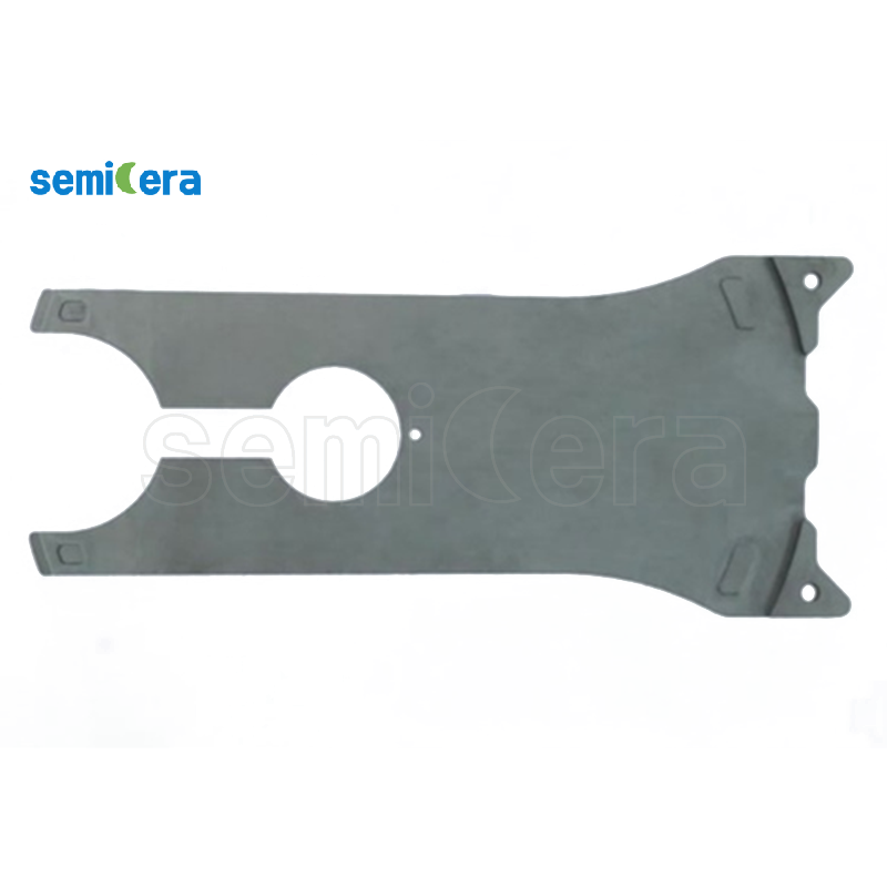
Wafer handling arm is a key equipment used in the semiconductor manufacturing process to handle, transfer and position wafers. It usually consists of a robotic arm, a gripper and a control system, with precise movement and positioning capabilities. Wafer handling arms are widely used in various links in semiconductor manufacturing, including process steps such as wafer loading, cleaning, thin film deposition, etching, lithography and inspection. Its precision, reliability and automation capabilities are essential to ensure the quality, efficiency and consistency of the production process.
The main functions of the wafer handling arm include:
1. Wafer transfer: The wafer handling arm is able to accurately transfer wafers from one location to another, such as taking wafers from a storage rack and placing them in a processing device.
2. Positioning and orientation: The wafer handling arm is able to accurately position and orient the wafer to ensure correct alignment and position for subsequent processing or measurement operations.
3. Clamping and releasing: Wafer handling arms are usually equipped with grippers that can safely clamp wafers and release them when needed to ensure safe transfer and handling of wafers.
4. Automated control: The wafer handling arm is equipped with an advanced control system that can automatically execute predetermined action sequences, improve production efficiency and reduce human errors.
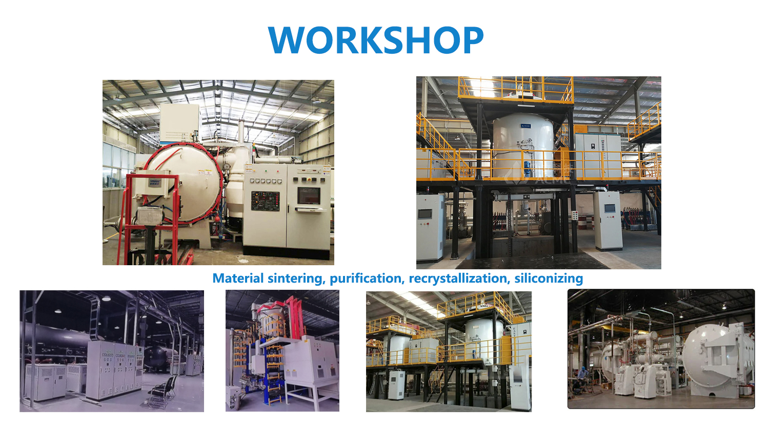
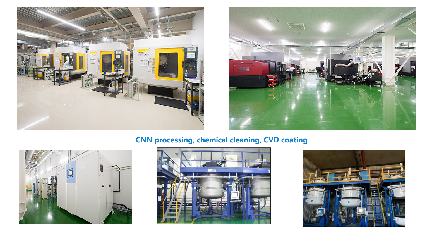
Characteristics and advantages
1.Precise dimensions and thermal stability.
2.High specific stiffness and excellent thermal uniformity, long-term use is not easy to bend deformation.
3.It has a smooth surface and good wear resistance, thus safely handling the chip without particle contamination.
4.Silicon carbide resistivity in 106-108Ω, non-magnetic, in line with anti-ESD specification requirements; It can prevent the accumulation of static electricity on the surface of the chip.
5.Good thermal conductivity, low expansion coefficient.