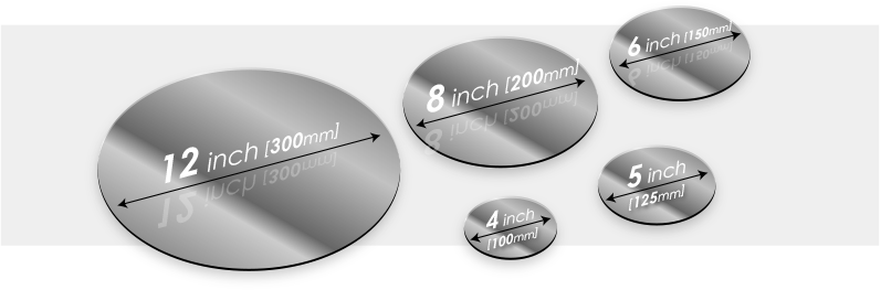
Semicera’s Wafer Cassette is a critical component in the semiconductor manufacturing process, designed to securely hold and transport delicate semiconductor wafers. The Wafer Cassette provides exceptional protection, ensuring that each wafer is kept free from contaminants and physical damage during handling, storage, and transportation.
Constructed with high-purity, chemical-resistant materials, the Semicera Wafer Cassette guarantees the highest levels of cleanliness and durability, essential for maintaining the integrity of wafers at every stage of production. The precision engineering of these cassettes allows for seamless integration with automated handling systems, minimizing the risk of contamination and mechanical damage.
The design of the Wafer Cassette also supports optimal airflow and temperature control, which is crucial for processes that require specific environmental conditions. Whether used in cleanrooms or during thermal processing, the Semicera Wafer Cassette is engineered to meet the stringent demands of the semiconductor industry, providing reliable and consistent performance to enhance manufacturing efficiency and product quality.
|
Items |
Production |
Research |
Dummy |
|
Crystal Parameters |
|||
|
Polytype |
4H |
||
|
Surface orientation error |
<11-20 >4±0.15° |
||
|
Electrical Parameters |
|||
|
Dopant |
n-type Nitrogen |
||
|
Resistivity |
0.015-0.025ohm·cm |
||
|
Mechanical Parameters |
|||
|
Diameter |
150.0±0.2mm |
||
|
Thickness |
350±25 μm |
||
|
Primary flat orientation |
[1-100]±5° |
||
|
Primary flat length |
47.5±1.5mm |
||
|
Secondary flat |
None |
||
|
TTV |
≤5 μm |
≤10 μm |
≤15 μm |
|
LTV |
≤3 μm(5mm*5mm) |
≤5 μm(5mm*5mm) |
≤10 μm(5mm*5mm) |
|
Bow |
-15μm ~ 15μm |
-35μm ~ 35μm |
-45μm ~ 45μm |
|
Warp |
≤35 μm |
≤45 μm |
≤55 μm |
|
Front(Si-face) roughness(AFM) |
Ra≤0.2nm (5μm*5μm) |
||
|
Structure |
|||
|
Micropipe density |
<1 ea/cm2 |
<10 ea/cm2 |
<15 ea/cm2 |
|
Metal impurities |
≤5E10atoms/cm2 |
NA |
|
|
BPD |
≤1500 ea/cm2 |
≤3000 ea/cm2 |
NA |
|
TSD |
≤500 ea/cm2 |
≤1000 ea/cm2 |
NA |
|
Front Quality |
|||
|
Front |
Si |
||
|
Surface finish |
Si-face CMP |
||
|
Particles |
≤60ea/wafer (size≥0.3μm) |
NA |
|
|
Scratches |
≤5ea/mm. Cumulative length ≤Diameter |
Cumulative length≤2*Diameter |
NA |
|
Orange peel/pits/stains/striations/ cracks/contamination |
None |
NA |
|
|
Edge chips/indents/fracture/hex plates |
None |
||
|
Polytype areas |
None |
Cumulative area≤20% |
Cumulative area≤30% |
|
Front laser marking |
None |
||
|
Back Quality |
|||
|
Back finish |
C-face CMP |
||
|
Scratches |
≤5ea/mm,Cumulative length≤2*Diameter |
NA |
|
|
Back defects (edge chips/indents) |
None |
||
|
Back roughness |
Ra≤0.2nm (5μm*5μm) |
||
|
Back laser marking |
1 mm (from top edge) |
||
|
Edge |
|||
|
Edge |
Chamfer |
||
|
Packaging |
|||
|
Packaging |
Epi-ready with vacuum packaging Multi-wafer cassette packaging |
||
|
*Notes: "NA" means no request Items not mentioned may refer to SEMI-STD. |
|||