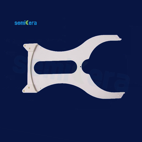
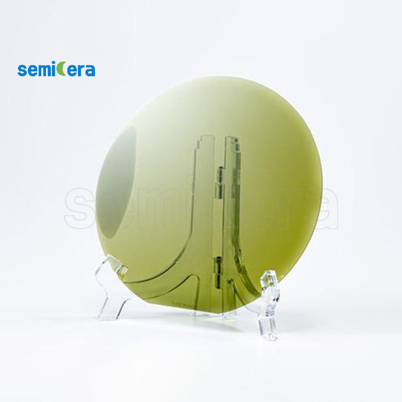
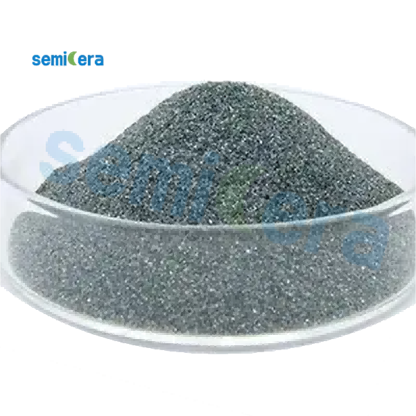
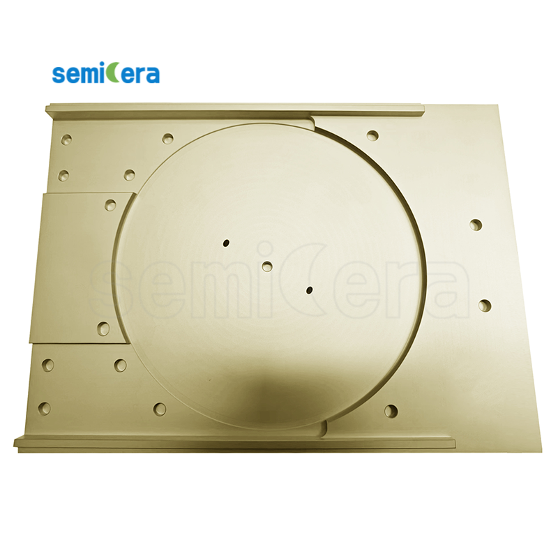
Semicera’s SiN Substrates are designed to meet the rigorous standards of today’s semiconductor industry, where reliability, thermal stability, and material purity are essential. Manufactured to deliver exceptional wear resistance, high thermal stability, and superior purity, Semicera’s SiN Substrates serve as a reliable solution across a variety of demanding applications. These substrates support precision performance in advanced semiconductor processing, making them ideal for a wide array of microelectronics and high-performance device applications.
Key Features of SiN Substrates
Semicera’s SiN Substrates stand out with their remarkable durability and resilience under high-temperature conditions. Their exceptional wear resistance and high thermal stability allow them to endure challenging manufacturing processes without performance degradation. The high purity of these substrates also reduces the risk of contamination, ensuring a stable and clean foundation for critical thin-film applications. This makes SiN Substrates a preferred choice in environments requiring high-quality material for reliable and consistent output.
Applications in the Semiconductor Industry
In the semiconductor industry, SiN Substrates are essential across multiple production stages. They play a vital role in supporting and insulating various materials, including Si Wafer, SOI Wafer, and SiC Substrate technologies. Semicera’s SiN substrates contribute to stable device performance, particularly when used as a base layer or insulating layer in multi-layer structures. Furthermore, SiN Substrates enable high-quality Epi-Wafer growth by providing a dependable, stable surface for epitaxial processes, making them invaluable for applications that demand precise layering, such as in microelectronics and optical components.
Versatility for Emerging Material Testing and Development
Semicera’s SiN Substrates are also versatile for testing and developing new materials, such as Gallium Oxide Ga2O3 and AlN Wafer. These substrates offer a reliable testing platform for evaluating performance characteristics, stability, and compatibility of these emerging materials, which are vital for the future of high-power and high-frequency devices. Additionally, Semicera’s SiN substrates are compatible with Cassette systems, enabling secure handling and transport across automated production lines, thus supporting efficiency and consistency in mass production environments.
Whether in high-temperature environments, advanced R&D, or the production of next-generation semiconductor materials, Semicera’s SiN Substrates provide robust reliability and adaptability. With their impressive wear resistance, thermal stability, and purity, Semicera’s SiN substrates are an indispensable choice for manufacturers aiming to optimize performance and maintain quality across various stages of semiconductor fabrication.


