Semicera is pleased to offer the PFA Cassette, a premium choice for wafer handling in environments where chemical resistance and durability are paramount. Crafted from high-purity Perfluoroalkoxy (PFA) material, this cassette is designed to withstand the most demanding conditions in semiconductor fabrication, ensuring the safety and integrity of your wafers.
Unmatched Chemical Resistance The PFA Cassette is engineered to provide superior resistance to a wide range of chemicals, making it the perfect choice for processes that involve aggressive acids, solvents, and other harsh chemicals. This robust chemical resistance ensures that the cassette remains intact and functional even in the most corrosive environments, thereby extending its lifespan and reducing the need for frequent replacements.
High-Purity Construction Semicera’s PFA Cassette is manufactured from ultra-pure PFA material, which is critical in preventing contamination during wafer processing. This high-purity construction minimizes the risk of particle generation and chemical leaching, ensuring that your wafers are protected from impurities that could compromise their quality.
Enhanced Durability and Performance Designed for durability, the PFA Cassette maintains its structural integrity under extreme temperatures and rigorous processing conditions. Whether exposed to high temperatures or subjected to repeated handling, this cassette retains its shape and performance, offering long-term reliability in demanding manufacturing environments.
Precision Engineering for Secure Handling The Semicera PFA Cassette features precise engineering that ensures secure and stable wafer handling. Each slot is carefully designed to hold wafers securely in place, preventing any movement or shifting that could result in damage. This precision engineering supports consistent and accurate wafer placement, contributing to overall process efficiency.
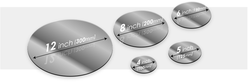
Versatile Application Across Processes Thanks to its superior material properties, the PFA Cassette is versatile enough to be used across various stages of semiconductor fabrication. It is particularly well-suited for wet etching, chemical vapor deposition (CVD), and other processes that involve harsh chemical environments. Its adaptability makes it an essential tool in maintaining process integrity and wafer quality.
Commitment to Quality and Innovation At Semicera, we are committed to providing products that meet the highest industry standards. The PFA Cassette exemplifies this commitment, offering a reliable solution that integrates seamlessly into your manufacturing processes. Each cassette undergoes strict quality control to ensure it meets our rigorous performance criteria, delivering the excellence you expect from Semicera.
|
Items |
Production |
Research |
Dummy |
|
Crystal Parameters |
|||
|
Polytype |
4H |
||
|
Surface orientation error |
<11-20 >4±0.15° |
||
|
Electrical Parameters |
|||
|
Dopant |
n-type Nitrogen |
||
|
Resistivity |
0.015-0.025ohm·cm |
||
|
Mechanical Parameters |
|||
|
Diameter |
150.0±0.2mm |
||
|
Thickness |
350±25 μm |
||
|
Primary flat orientation |
[1-100]±5° |
||
|
Primary flat length |
47.5±1.5mm |
||
|
Secondary flat |
None |
||
|
TTV |
≤5 μm |
≤10 μm |
≤15 μm |
|
LTV |
≤3 μm(5mm*5mm) |
≤5 μm(5mm*5mm) |
≤10 μm(5mm*5mm) |
|
Bow |
-15μm ~ 15μm |
-35μm ~ 35μm |
-45μm ~ 45μm |
|
Warp |
≤35 μm |
≤45 μm |
≤55 μm |
|
Front(Si-face) roughness(AFM) |
Ra≤0.2nm (5μm*5μm) |
||
|
Structure |
|||
|
Micropipe density |
<1 ea/cm2 |
<10 ea/cm2 |
<15 ea/cm2 |
|
Metal impurities |
≤5E10atoms/cm2 |
NA |
|
|
BPD |
≤1500 ea/cm2 |
≤3000 ea/cm2 |
NA |
|
TSD |
≤500 ea/cm2 |
≤1000 ea/cm2 |
NA |
|
Front Quality |
|||
|
Front |
Si |
||
|
Surface finish |
Si-face CMP |
||
|
Particles |
≤60ea/wafer (size≥0.3μm) |
NA |
|
|
Scratches |
≤5ea/mm. Cumulative length ≤Diameter |
Cumulative length≤2*Diameter |
NA |
|
Orange peel/pits/stains/striations/ cracks/contamination |
None |
NA |
|
|
Edge chips/indents/fracture/hex plates |
None |
||
|
Polytype areas |
None |
Cumulative area≤20% |
Cumulative area≤30% |
|
Front laser marking |
None |
||
|
Back Quality |
|||
|
Back finish |
C-face CMP |
||
|
Scratches |
≤5ea/mm,Cumulative length≤2*Diameter |
NA |
|
|
Back defects (edge chips/indents) |
None |
||
|
Back roughness |
Ra≤0.2nm (5μm*5μm) |
||
|
Back laser marking |
1 mm (from top edge) |
||
|
Edge |
|||
|
Edge |
Chamfer |
||
|
Packaging |
|||
|
Packaging |
Epi-ready with vacuum packaging Multi-wafer cassette packaging |
||
|
*Notes: "NA" means no request Items not mentioned may refer to SEMI-STD. |
|||