-

Seed Crystal Preparation Process in SiC Single Crystal Growth
Silicon carbide (SiC) material has the advantages of a wide bandgap, high thermal conductivity, high critical breakdown field strength, and high saturated electron drift velocity, making it highly promising in the semiconductor manufacturing field. SiC single crystals are generally produced throu...Read more -
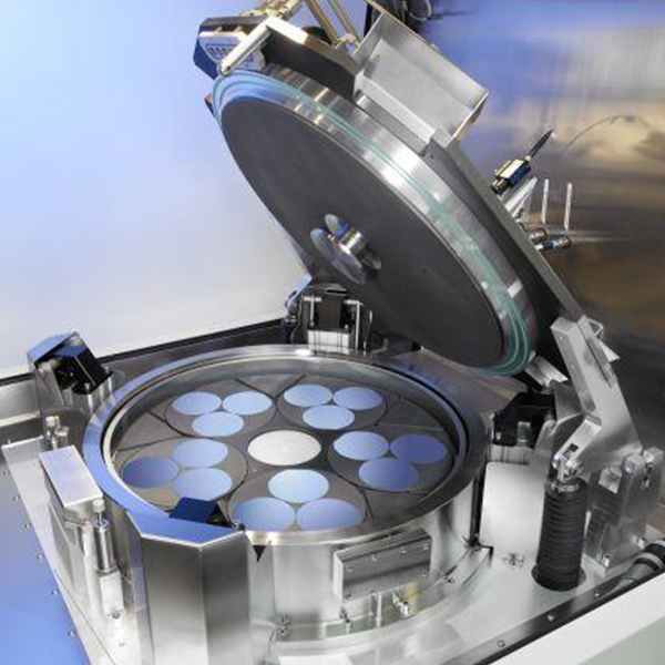
What are the methods for wafer polishing?
Of all the processes involved in creating a chip, the final fate of the wafer is to be cut into individual dies and packaged in small, enclosed boxes with only a few pins exposed. The chip will be evaluated based on its threshold, resistance, current, and voltage values, but no one will consider ...Read more -
The Basic Introduction of SiC Epitaxial Growth Process
Epitaxial layer is a specific single crystal film grown on the wafer by ep·itaxial process, and the substrate wafer and epitaxial film are called epitaxial wafer. By growing the silicon carbide epitaxial layer on the conductive silicon carbide substrate, the silicon carbide homogeneous epitaxial...Read more -
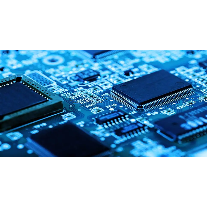
Key points of semiconductor packaging process quality control
Key Points for Quality Control in Semiconductor Packaging ProcessCurrently, the process technology for semiconductor packaging has significantly improved and optimized. However, from an overall perspective, the processes and methods for semiconductor packaging have not yet reached the most perfec...Read more -
Challenges in Semiconductor Packaging Process
The current techniques for semiconductor packaging are gradually improving, but the extent to which automated equipment and technologies are adopted in semiconductor packaging directly determines the realization of expected outcomes. The existing semiconductor packaging processes still suffer fro...Read more -
Research and Analysis of Semiconductor Packaging Process
Overview of Semiconductor Process The semiconductor process primarily involves applying microfabrication and film technologies to fully connect chips and other elements within various regions, such as substrates and frames. This facilitates the extraction of lead terminals and encapsulation with ...Read more -
New Trends in the Semiconductor Industry: The Application of Protective Coating Technology
The semiconductor industry is witnessing unprecedented growth, especially in the realm of silicon carbide (SiC) power electronics. With many large-scale wafer fabs undergoing construction or expansion to meet the surging demand for SiC devices in electric vehicles, this ...Read more -
What are the main steps in the processing of SiC substrates?
How we produce-processing steps for SiC substrates are as follows: 1. Crystal Orientation: Using X-ray diffraction to orient the crystal ingot. When an X-ray beam is directed at the desired crystal face, the angle of the diffracted beam determines the crystal orienta...Read more -

An important material that determines the quality of single crystal silicon growth – thermal field
The growth process of single crystal silicon is completely carried out in the thermal field. A good thermal field is conducive to improving crystal quality and has high crystallization efficiency. The design of the thermal field largely determines the changes and changes...Read more -
What is epitaxial growth?
Epitaxial growth is a technology that grows a single crystal layer on a single crystal substrate (substrate) with the same crystal orientation as the substrate, as if the original crystal has extended outward. This newly grown single crystal layer can be different from the substrate in terms of c...Read more -

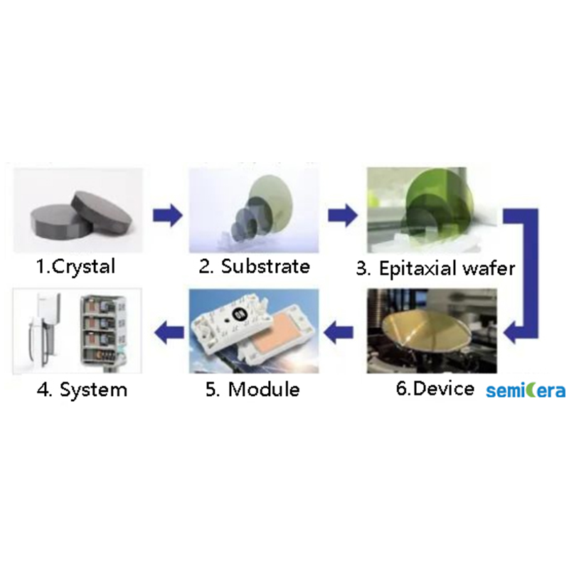
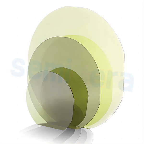
What is the difference between substrate and epitaxy?
In the wafer preparation process, there are two core links: one is the preparation of the substrate, and the other is the implementation of the epitaxial process. The substrate, a wafer carefully crafted from semiconductor single crystal material, can be directly put into the wafer manufacturing ...Read more -

Unveiling the Versatile Characteristics of Graphite Heaters
Graphite heaters have emerged as indispensable tools across various industries due to their exceptional properties and versatility. From laboratories to industrial settings, these heaters play a pivotal role in processes ranging from material synthesis to analytical techniques. Among the various ...Read more