Rolling refers to the process of grinding the outer diameter of a silicon single crystal rod into a single crystal rod of the required diameter using a diamond grinding wheel, and grinding out a flat edge reference surface or positioning groove of the single crystal rod.
The outer diameter surface of the single crystal rod prepared by the single crystal furnace is not smooth and flat, and its diameter is larger than the diameter of the silicon wafer used in the final application. The required rod diameter can be obtained by rolling the outer diameter.
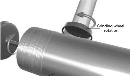
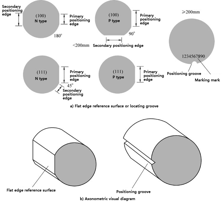
The rolling mill has the function of grinding the flat edge reference surface or positioning groove of the silicon single crystal rod, that is, to perform directional testing on the single crystal rod with the required diameter. On the same rolling mill equipment, the flat edge reference surface or positioning groove of the single crystal rod is ground. Generally, single crystal rods with a diameter of less than 200mm use flat edge reference surfaces, and single crystal rods with a diameter of 200mm and above use positioning grooves. Single crystal rods with a diameter of 200mm can also be made with flat edge reference surfaces as needed. The purpose of the single crystal rod orientation reference surface is to meet the needs of automated positioning operation of process equipment in integrated circuit manufacturing; to indicate the crystal orientation and conductivity type of the silicon wafer, etc., to facilitate production management; the main positioning edge or positioning groove is perpendicular to the <110> direction. During the chip packaging process, the dicing process can cause natural cleavage of the wafer, and positioning can also prevent the generation of fragments.
The main purposes of the rounding process include: Improving surface quality: Rounding can remove burrs and unevenness on the surface of silicon wafers and improve the surface smoothness of silicon wafers, which is very important for subsequent photolithography and etching processes. Reducing stress: Stress may be generated during the cutting and processing of silicon wafers. Rounding can help release these stresses and prevent the silicon wafers from breaking in subsequent processes. Improving the mechanical strength of silicon wafers: During the rounding process, the edges of the silicon wafers will become smoother, which helps to improve the mechanical strength of the silicon wafers and reduce damage during transportation and use. Ensuring dimensional accuracy: By rounding, the dimensional accuracy of silicon wafers can be ensured, which is crucial for the manufacture of semiconductor devices. Improving the electrical properties of silicon wafers: The edge processing of silicon wafers has an important influence on their electrical properties. Rounding can improve the electrical properties of silicon wafers, such as reducing leakage current. Aesthetics: The edges of silicon wafers are smoother and more beautiful after rounding, which is also necessary for certain application scenarios.
Post time: Jul-30-2024