In the semiconductor industry chain, especially in the third-generation semiconductor (wide bandgap semiconductor) industry chain, there are substrates and epitaxial layers. What is the significance of the epitaxial layer? What is the difference between the substrate and the substrate?
The substrate is a wafer made of semiconductor single crystal materials. The substrate can directly enter the wafer manufacturing link to produce semiconductor devices, or it can be processed by epitaxial process to produce epitaxial wafers. The substrate is the bottom of the wafer (cut the wafer, you can get one die after another, and then package it to become the legendary chip) (in fact, the bottom of the chip is generally plated with a layer of back gold, used as a “ground” connection, but it is made in the back process), and the base that carries the entire support function (the skyscraper in the chip is built on the substrate).
Epitaxy refers to the process of growing a new single crystal on a single crystal substrate that has been carefully processed by cutting, grinding, polishing, etc. The new single crystal can be the same material as the substrate, or it can be a different material (homoepitaxial or heteroepitaxial).
Since the newly formed single crystal layer grows along the substrate crystal phase, it is called an epitaxial layer (usually several microns thick. Take silicon as an example: the meaning of silicon epitaxial growth is to grow a layer of crystal with good lattice structure integrity on a silicon single crystal substrate with a certain crystal orientation and different resistivity and thickness as the substrate), and the substrate with the epitaxial layer is called an epitaxial wafer (epitaxial wafer = epitaxial layer + substrate). Device manufacturing is carried out on the epitaxial layer.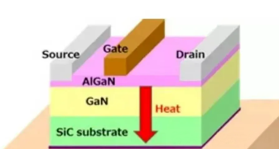
Epitaxiality is divided into homoepitaxiality and heteroepitaxiality. Homoepitaxiality is to grow an epitaxial layer of the same material as the substrate on the substrate. What is the significance of homoepitaxiality? – Improve product stability and reliability. Although homoepitaxiality is to grow an epitaxial layer of the same material as the substrate, although the material is the same, it can improve the material purity and uniformity of the wafer surface. Compared with the polished wafers processed by mechanical polishing, the substrate processed by epitaxiality has high surface flatness, high cleanliness, fewer micro defects, and fewer surface impurities. Therefore, the resistivity is more uniform, and it is easier to control surface defects such as surface particles, stacking faults, and dislocations. Epitaxy not only improves product performance, but also ensures product stability and reliability.
What are the benefits of making another layer of silicon atoms epitaxial on the silicon wafer substrate? In the CMOS silicon process, epitaxial growth (EPI, epitaxial) on the wafer substrate is a very critical process step.
1. Improve crystal quality
Initial substrate defects and impurities: The wafer substrate may have certain defects and impurities during the manufacturing process. The growth of the epitaxial layer can generate a high-quality, low-defect and impurity-concentration single-crystalline silicon layer on the substrate, which is very important for subsequent device manufacturing. Uniform crystal structure: Epitaxial growth can ensure a more uniform crystal structure, reduce the influence of grain boundaries and defects in the substrate material, and thus improve the crystal quality of the entire wafer.
2. Improve electrical performance
Optimize device characteristics: By growing an epitaxial layer on the substrate, the doping concentration and type of silicon can be precisely controlled to optimize the electrical performance of the device. For example, the doping of the epitaxial layer can accurately adjust the threshold voltage and other electrical parameters of the MOSFET. Reduce leakage current: High-quality epitaxial layers have lower defect density, which helps reduce leakage current in the device, thereby improving the performance and reliability of the device.
3. Support advanced process nodes
Reducing feature size: In smaller process nodes (such as 7nm, 5nm), device feature size continues to shrink, requiring more refined and high-quality materials. Epitaxial growth technology can meet these requirements and support high-performance and high-density integrated circuit manufacturing. Improve breakdown voltage: The epitaxial layer can be designed to have a higher breakdown voltage, which is critical for manufacturing high-power and high-voltage devices. For example, in power devices, the epitaxial layer can increase the breakdown voltage of the device and increase the safe operating range.
4. Process compatibility and multi-layer structure
Multi-layer structure: Epitaxial growth technology allows multi-layer structures to be grown on a substrate, and different layers can have different doping concentrations and types. This is very helpful for manufacturing complex CMOS devices and achieving three-dimensional integration. Compatibility: The epitaxial growth process is highly compatible with existing CMOS manufacturing processes and can be easily integrated into existing manufacturing processes without significantly modifying the process lines.
Post time: Jul-16-2024