Most engineers are unfamiliar with epitaxy, which plays an important role in semiconductor device manufacturing. Epitaxy can be used in different chip products, and different products have different types of epitaxy, including Si epitaxy, SiC epitaxy, GaN epitaxy, etc.
What is epitaxy?
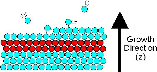
Epitaxy is often called “Epitaxy” in English. The word comes from the Greek words “epi” (meaning “above”) and “taxis” (meaning “arrangement”). As the name suggests, it means arranging neatly on top of an object. The epitaxy process is to deposit a thin single crystal layer on a single crystal substrate. This newly deposited single crystal layer is called an epitaxial layer.
There are two main types of epitaxy: homoepitaxial and heteroepitaxial. Homoepitaxial refers to growing the same material on the same type of substrate. The epitaxial layer and the substrate have exactly the same lattice structure. Heteroepitaxy is the growth of another material on a substrate of one material. In this case, the lattice structure of the epitaxially grown crystal layer and the substrate may be different. What are single crystals and polycrystalline?
In semiconductors, we often hear the terms single crystal silicon and polycrystalline silicon. Why are some silicon called single crystals and some silicon called polycrystalline?
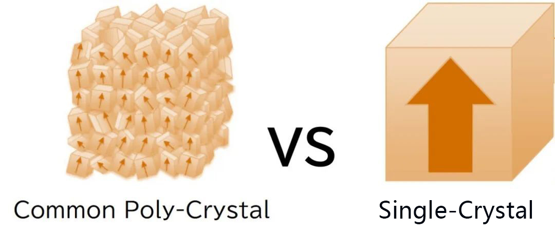
Single crystal: The lattice arrangement is continuous and unchanged, without grain boundaries, that is, the entire crystal is composed of a single lattice with consistent crystal orientation. Polycrystalline: Polycrystalline is composed of many small grains, each of which is a single crystal, and their orientations are random with respect to each other. These grains are separated by grain boundaries. The production cost of polycrystalline materials is lower than that of single crystals, so they are still useful in some applications. Where will the epitaxial process be involved?
In the manufacture of silicon-based integrated circuits, the epitaxial process is widely used. For example, silicon epitaxy is used to grow a pure and finely controlled silicon layer on a silicon substrate, which is extremely important for the manufacture of advanced integrated circuits. In addition, in power devices, SiC and GaN are two commonly used wide bandgap semiconductor materials with excellent power handling capabilities. These materials are usually grown on silicon or other substrates through epitaxy. In quantum communication, semiconductor-based quantum bits usually use silicon germanium epitaxial structures. Etc.
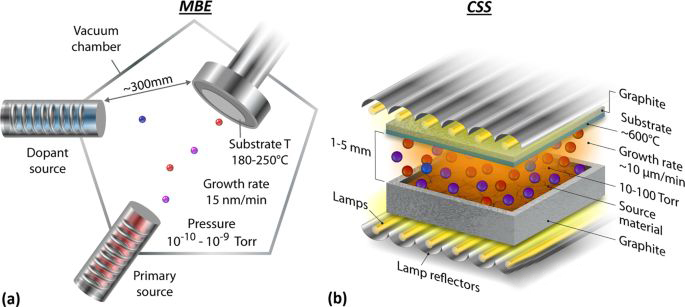
Methods of epitaxial growth?
Three commonly used semiconductor epitaxy methods:
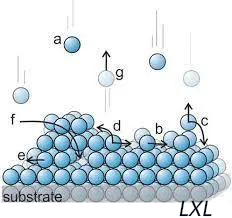
Molecular beam epitaxy (MBE): Molecular beam epitaxy) is a semiconductor epitaxial growth technology performed under ultra-high vacuum conditions. In this technology, the source material is evaporated in the form of atoms or molecular beams and then deposited on a crystalline substrate. MBE is a very precise and controllable semiconductor thin film growth technology that can precisely control the thickness of the deposited material at the atomic level.
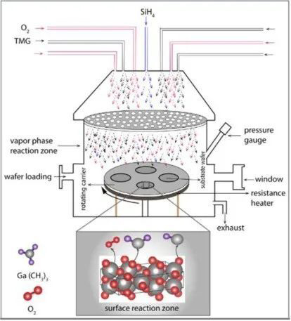
Metal organic CVD (MOCVD): In the MOCVD process, organic metals and hydride gases containing the required elements are supplied to the substrate at an appropriate temperature, and the required semiconductor materials are generated through chemical reactions and deposited on the substrate, while the remaining compounds and reaction products are discharged.

Vapor Phase Epitaxy (VPE): Vapor Phase Epitaxy is an important technology commonly used in the production of semiconductor devices. Its basic principle is to transport the vapor of a single substance or compound in a carrier gas and deposit crystals on a substrate through chemical reactions.
Post time: Aug-06-2024