What is CVD coating?
Chemical Vapor Deposition (CVD) coating is a high-precision surface modification process that produces a solid film coating by reacting gaseous chemical precursors on a heated or plasma-activated substrate surface. The process is as follows:
1. Gaseous precursors (e.g. methane, silane) are introduced into the reaction chamber;
2. The gas molecules react or decompose at high temperatures (500-1,200°C) or under plasma activation;
3. The resulting solid material adheres to the surface of the substrate in an atomic level bond to form a homogeneous coating.
Core features of CVD Coating:
● Coating thickness can be controlled in the nanometer to micron range;
● Applicable to ceramics (e.g., titanium nitride TiN, aluminum oxide Al₂O₃), carbides (e.g., silicon carbide SiC), diamonds and metals;
● Excellent conformal coverage of substrates with complex geometries.
Examples of typical reactions:
● Tungsten deposition: WF6 + 3H2 → W(Solid) + 6HF(Gas)
● Titanium nitride deposition: TiCl4 + 1/2N2 + 2H2 → TiN(Solid) + 4HCl(Gas)
Process temperatures are typically 600-1100°C, which can be reduced to 300-500°C by plasma assisted (PACVD).

Core Benefits of CVD Coatings
● Superior adhesion: Atomic bonding ensures that the coating is resistant to peeling under stress.
● Uniform coverage: Perfect fit to complex shapes (e.g. internal recesses, sharp edges).
● High purity: Avoids the problems of impurities common in the PVD method.
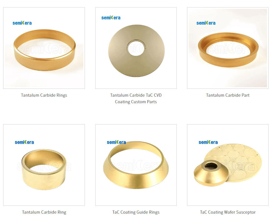
● High temperature resistance: Withstands up to 2,200°C (e.g. Tantalum Carbide coatings).
● Chemically inert: Resistant to oxidation, acids and corrosive environments.
● Cost-effective: Significantly reduces long-term maintenance and replacement costs for industrial tools.
The role of CVD SiC coatings in semiconductor manufacturing
Due to SiC’s excellent high temperature resistance, high thermal conductivity, chemical inertness and low coefficient of thermal expansion, CVD SiC coated products are widely used in semiconductor manufacturing processes, and the main application areas are as follows:
1. Wafer processing equipment
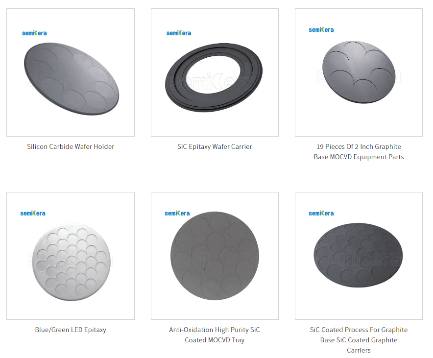
-Wafer boat and Wafer Carrier: SiC coated wafer carriers are able to withstand high temperature of 1350/ 1650°C and surface roughness <10μm in PECVD process.
-Reaction Chamber Components: CZ method monocrystalline silicon growth reflectors to reduce metal contamination and improve thermal uniformity.
Real-world examples:
After adopting Semicera’s CVD SiC boat in 12-inch wafer fab, the lifetime of the boat in high temperature process has been increased from 300 times to 5,000 times, and the annual maintenance cost has been reduced by 62%.
2.Epitaxial Process
-SiC Epitaxial Deposition: 4H-SiC homogeneous epitaxial growth in fluidized bed reactor as substrate protection layer.
-SiC Epitaxial substrate:As a key component in the Epitaxial growth process, SiC Epitaxial substrate is usually used to carry the silicon substrate and realize the uniform deposition of single crystal film at high temperature. Silicon Carbide (SiC) coated substrates processed by Chemical Vapor Deposition (CVD) have a coefficient of thermal expansion of only 4.3×10⁻⁶/K (100-600°C), so they can be effectively matched to silicon wafers to reduce stress. It is an irreplaceable process component in advanced semiconductor manufacturing.
3.High temperature processing system
-Diffusion Furnace Tube: Combined with the statistical data in actual production, Semicera’s Diffusion furnace tube can withstand 1200℃ water-oxygen environment in thermal oxidation process, and the life span has been extended by 3 times, which greatly improves the life cycle of the product.
-MOCVD nozzle: Improved resistance to plasma corrosion and reduced particle contamination in AIGaN epitaxy.
Post time: Mar-31-2025

