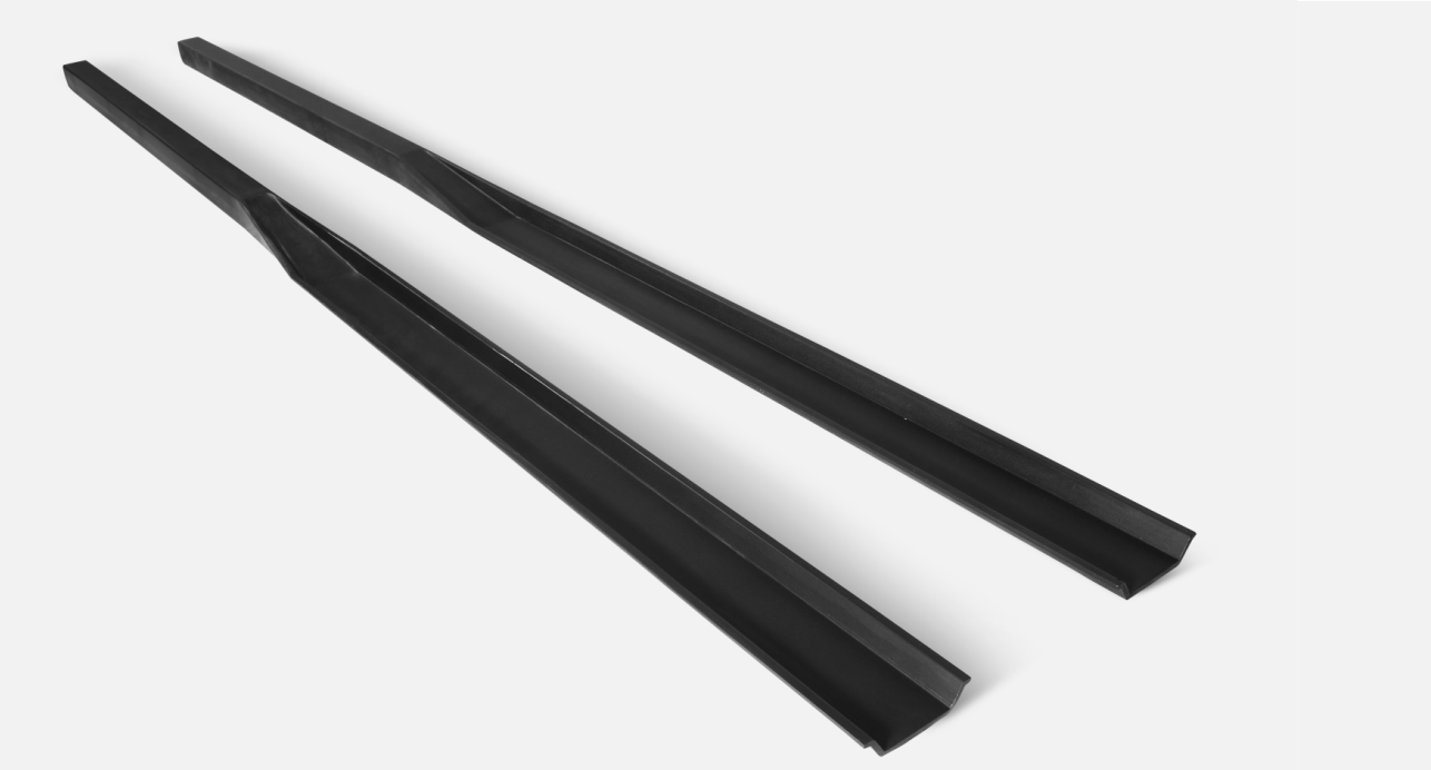
In the realm of semiconductor manufacturing, the wafer paddle plays a pivotal role in ensuring efficient and precise handling of wafers during various processes. It is mainly used in the (diffusion) coating process of polycrystalline silicon wafers or monocrystalline silicon wafers in the diffusion furnace to carry and transport silicon wafers in a high temperature environment.
Semicera is proud to introduce its state of the art wafer paddles, designed to enhance operational efficiency in applications involving CVD SiC.
The wafer paddle serves as a crucial component in the semiconductor fabrication process, providing the necessary support for wafers during chemical vapor deposition (CVD) and other critical steps. With Semicera’s advanced engineering, these paddles ensure optimal alignment and stability, reducing the risk of defects and improving overall yield. Our commitment to innovation means that each paddle is crafted with precision to meet the rigorous demands of the industry.
Semicera’s wafer paddles are specifically designed for compatibility with various coating processes, including CVD SiC and TAC coating. The integration of high-quality materials ensures durability and reliability, making them ideal for high-temperature environments. By utilizing Semicera’s wafer paddles, manufacturers can achieve superior results while maintaining stringent quality standards.
In summary, the wafer paddle from Semicera is an essential tool for semiconductor production, enhancing both efficiency and reliability in wafer handling. As we continue to innovate and expand our product offerings, Semicera remains dedicated to providing cutting-edge solutions that meet the evolving needs of the semiconductor industry.
Post time: Sep-25-2024