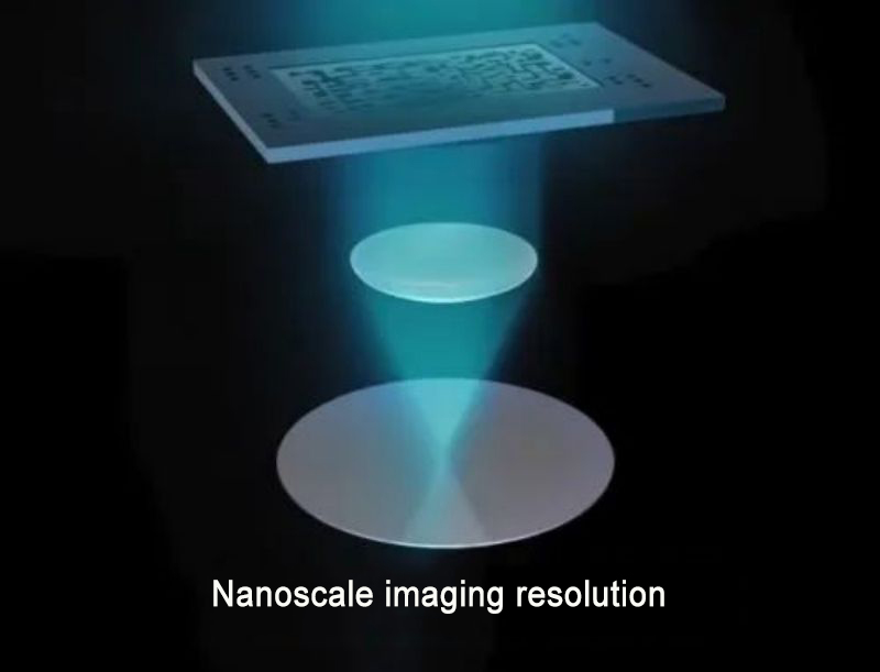
Of all the processes involved in creating a chip, the final fate of the wafer is to be cut into individual dies and packaged in small, enclosed boxes with only a few pins exposed. The chip will be evaluated based on its threshold, resistance, current, and voltage values, but no one will consider its appearance. During the manufacturing process, we repeatedly polish the wafer to achieve the necessary planarization, especially for each photolithography step. The wafer surface must be extremely flat because, as the chip manufacturing process shrinks, the lens of the photolithography machine needs to achieve nanometer-scale resolution by increasing the numerical aperture (NA) of the lens. However, this simultaneously reduces the depth of focus (DoF). The depth of focus refers to the depth within which the optical system can maintain focus. To ensure that the photolithography image remains clear and in focus, the surface variations of the wafer must fall within the depth of focus.
In simple terms, the photolithography machine sacrifices focusing ability to improve imaging precision. For instance, the new generation EUV photolithography machines have a numerical aperture of 0.55, but the vertical depth of focus is only 45 nanometers, with an even smaller optimal imaging range during photolithography. If the wafer is not flat, has uneven thickness, or surface undulations, it will cause issues during photolithography at the high and low points.
Photolithography is not the only process requiring a smooth wafer surface. Many other chip manufacturing processes also require wafer polishing. For example, after wet etching, polishing is needed to smooth the rough surface for subsequent coating and deposition. After shallow trench isolation (STI), polishing is required to smooth the excess silicon dioxide and complete the trench filling. After metal deposition, polishing is needed to remove excess metal layers and prevent device short circuits.
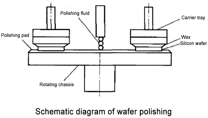
Therefore, the birth of a chip involves numerous polishing steps to reduce the wafer’s roughness and surface variations and to remove excess material from the surface. Additionally, surface defects caused by various process issues on the wafer often only become apparent after each polishing step. Thus, the engineers responsible for polishing hold significant responsibility. They are the central figures in the chip manufacturing process and often bear the blame in production meetings. They must be proficient in both wet etching and physical output, as the main polishing techniques in chip manufacturing.
What are the wafer polishing methods?
Polishing processes can be classified into three major categories based on the interaction principles between the polishing liquid and the silicon wafer surface:
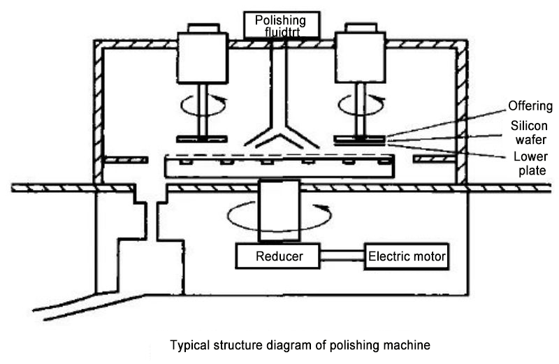
1. Mechanical Polishing Method:
Mechanical polishing removes the polished surface’s protrusions through cutting and plastic deformation to achieve a smooth surface. Common tools include oil stones, wool wheels, and sandpaper, primarily operated by hand. Special parts, such as the surfaces of rotating bodies, can use turntables and other auxiliary tools. For surfaces with high-quality requirements, super-fine polishing methods can be employed. Super-fine polishing uses specially made abrasive tools, which, in an abrasive-containing polishing liquid, are tightly pressed against the surface of the workpiece and rotated at high speed. This technique can achieve a surface roughness of Ra0.008μm, the highest among all polishing methods. This method is commonly used for optical lens molds.
2. Chemical Polishing Method:
Chemical polishing involves the preferential dissolution of the micro-protrusions on the material surface in a chemical medium, resulting in a smooth surface. The main advantages of this method are the lack of need for complex equipment, the ability to polish complex-shaped workpieces, and the capability to polish many workpieces simultaneously with high efficiency. The core issue of chemical polishing is the formulation of the polishing liquid. The surface roughness achieved by chemical polishing is typically several tens of micrometers.
3. Chemical Mechanical Polishing (CMP) Method:
Each of the first two polishing methods has its unique advantages. Combining these two methods can achieve complementary effects in the process. Chemical mechanical polishing combines mechanical friction and chemical corrosion processes. During CMP, the chemical reagents in the polishing liquid oxidize the polished substrate material, forming a soft oxide layer. This oxide layer is then removed through mechanical friction. Repeating this oxidation and mechanical removal process achieves effective polishing.
Current Challenges and Issues in Chemical Mechanical Polishing (CMP):
CMP faces several challenges and issues in the areas of technology, economics, and environmental sustainability:
1) Process Consistency: Achieving high consistency in the CMP process remains challenging. Even within the same production line, minor variations in process parameters between different batches or equipment can affect the final product’s consistency.
2) Adaptability to New Materials: As new materials continue to emerge, CMP technology must adapt to their characteristics. Some advanced materials may not be compatible with traditional CMP processes, requiring the development of more adaptable polishing liquids and abrasives.
3) Size Effects: As semiconductor device dimensions continue to shrink, issues caused by size effects become more significant. Smaller dimensions require higher surface flatness, necessitating more precise CMP processes.
4) Material Removal Rate Control: In some applications, precise control of the material removal rate for different materials is crucial. Ensuring consistent removal rates across various layers during CMP is essential for manufacturing high-performance devices.
5) Environmental Friendliness: The polishing liquids and abrasives used in CMP may contain environmentally harmful components. Research and development of more environmentally friendly and sustainable CMP processes and materials are important challenges.
6) Intelligence and Automation: While the intelligence and automation level of CMP systems are gradually improving, they must still cope with complex and variable production environments. Achieving higher levels of automation and intelligent monitoring to improve production efficiency is a challenge that needs to be addressed.
7) Cost Control: CMP involves high equipment and material costs. Manufacturers need to improve process performance while striving to reduce production costs to maintain market competitiveness.
Post time: Jun-05-2024