The cleanliness of the wafer surface will greatly affect the qualification rate of subsequent semiconductor processes and products. Up to 50% of all yield losses are caused by wafer surface contamination.
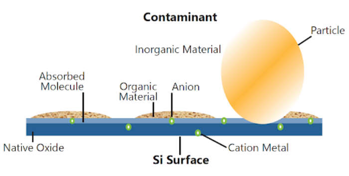
Objects that can cause uncontrolled changes in the electrical performance of the device or the device manufacturing process are collectively referred to as contaminants. Contaminants may come from the wafer itself, the clean room, process tools, process chemicals or water. Wafer contamination can generally be detected by visual observation, process inspection, or the use of complex analytical equipment in the final device test.
▲Contaminants on the surface of silicon wafers | Image source network
The results of contamination analysis can be used to reflect the degree and type of contamination encountered by the wafer in a certain process step, a specific machine or the overall process. According to the classification of detection methods, wafer surface contamination can be divided into the following types.
Metal contamination
Contamination caused by metals can cause semiconductor device defects of varying degrees.
Alkali metals or alkaline earth metals (Li, Na, K, Ca, Mg, Ba, etc.) can cause leakage current in the p-n structure, which in turn leads to the breakdown voltage of the oxide; transition metal and heavy metal (Fe, Cr, Ni, Cu, Au, Mn, Pb, etc.) pollution can reduce the carrier life cycle, reduce the service life of the component or increase the dark current when the component is working.
Common methods for detecting metal contamination are total reflection X-ray fluorescence, atomic absorption spectroscopy and inductively coupled plasma mass spectrometry (ICP-MS).
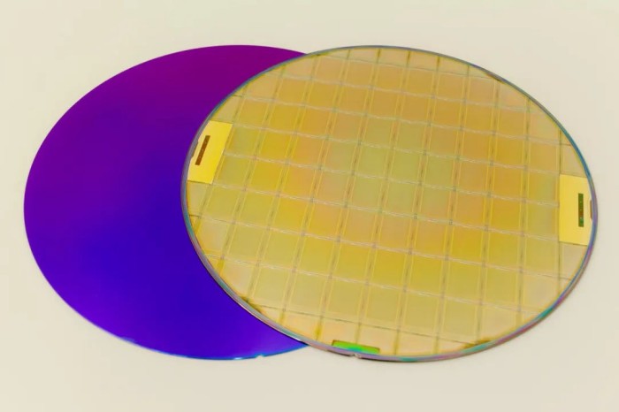
▲ Wafer surface contamination | ResearchGate
Metal contamination may come from reagents used in cleaning, etching, lithography, deposition, etc., or from the machines used in the process, such as ovens, reactors, ion implantation, etc., or it may be caused by careless wafer handling.
Particle contamination
Actual material deposits are usually observed by detecting light scattered from surface defects. Therefore, the more accurate scientific name for particle contamination is light-point defect. Particle contamination can cause blocking or masking effects in etching and lithography processes.
During film growth or deposition, pinholes and microvoids are generated, and if the particles are large and conductive, they can even cause short circuits.
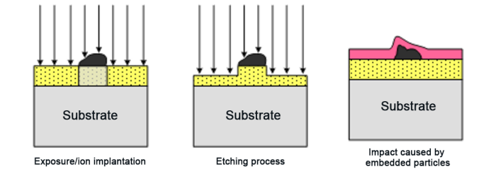
▲ Formation of particle contamination | Image source network
Tiny particle contamination can cause shadows on the surface, such as during photolithography. If large particles are located between the photomask and the photoresist layer, they can reduce the resolution of contact exposure.
In addition, they can block accelerated ions during ion implantation or dry etching. Particles may also be enclosed by the film, so that there are bumps and bumps. Subsequent deposited layers may crack or resist accumulation at these locations, causing problems during exposure.
Organic contamination
Contaminants containing carbon, as well as bonding structures associated with C, are called organic contamination. Organic contaminants may cause unexpected hydrophobic properties on the wafer surface, increase surface roughness, produce a hazy surface, disrupt epitaxial layer growth, and affect the cleaning effect of metal contamination if the contaminants are not removed first.
Such surface contamination is generally detected by instruments such as thermal desorption MS, X-ray photoelectron spectroscopy, and Auger electron spectroscopy.
▲Image source network
Gaseous contamination and water contamination
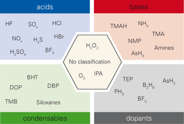
Atmospheric molecules and water contamination with molecular size are usually not removed by ordinary high-efficiency particulate air (HEPA) or ultra-low penetration air filters (ULPA). Such contamination is usually monitored by ion mass spectrometry and capillary electrophoresis.
Some contaminants may belong to multiple categories, for example, particles may be composed of organic or metallic materials, or both, so this type of contamination may also be classified as other types.
▲Gaseous molecular contaminants | IONICON
In addition, wafer contamination can also be classified as molecular contamination, particle contamination, and process-derived debris contamination according to the size of the contamination source. The smaller the size of the contamination particle, the more difficult it is to remove. In today's electronic component manufacturing, wafer cleaning procedures account for 30% - 40% of the entire production process.
▲Contaminants on the surface of silicon wafers | Image source network
Post time: Nov-18-2024


