Ion implantation is a method of adding a certain amount and type of impurities into semiconductor materials to change their electrical properties. The amount and distribution of impurities can be precisely controlled.
Part 1
Why use ion implantation process
In the manufacture of power semiconductor devices, the P/N region doping of traditional silicon wafers can be achieved by diffusion. However, the diffusion constant of impurity atoms in silicon carbide is extremely low, so it is unrealistic to achieve selective doping by diffusion process, as shown in Figure 1. On the other hand, the temperature conditions of ion implantation are lower than those of diffusion process, and a more flexible and accurate doping distribution can be formed.
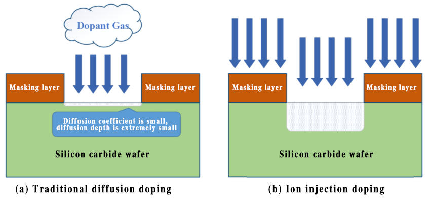
Figure 1 Comparison of diffusion and ion implantation doping technologies in silicon carbide materials
Part 2
How to achieve silicon carbide ion implantation
The typical high-energy ion implantation equipment used in the silicon carbide process manufacturing process mainly consists of an ion source, plasma, aspiration components, analytical magnets, ion beams, acceleration tubes, process chambers, and scanning disks, as shown in Figure 2.
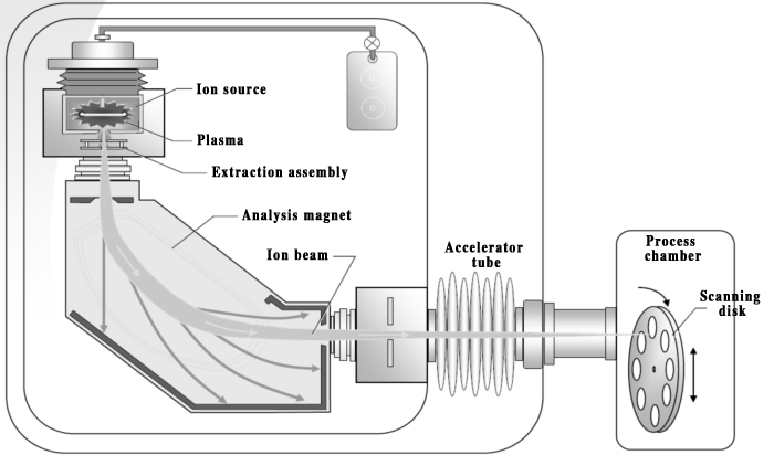
Figure 2 Schematic diagram of silicon carbide high-energy ion implantation equipment
(Source: “Semiconductor Manufacturing Technology”)
SiC ion implantation is usually carried out at high temperature, which can minimize the damage to the crystal lattice caused by ion bombardment. For 4H-SiC wafers, the production of N-type areas is usually achieved by implanting nitrogen and phosphorus ions, and the production of P-type areas is usually achieved by implanting aluminum ions and boron ions.
Table 1. Example of selective doping in SiC device manufacturing
(Source: Kimoto, Cooper, Fundamentals of Silicon Carbide Technology: Growth, Characterization, Devices, and Applications)
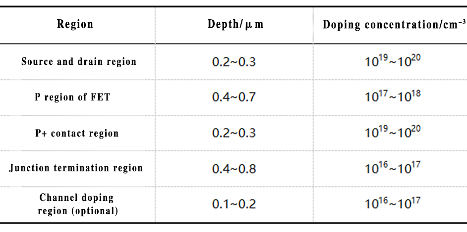
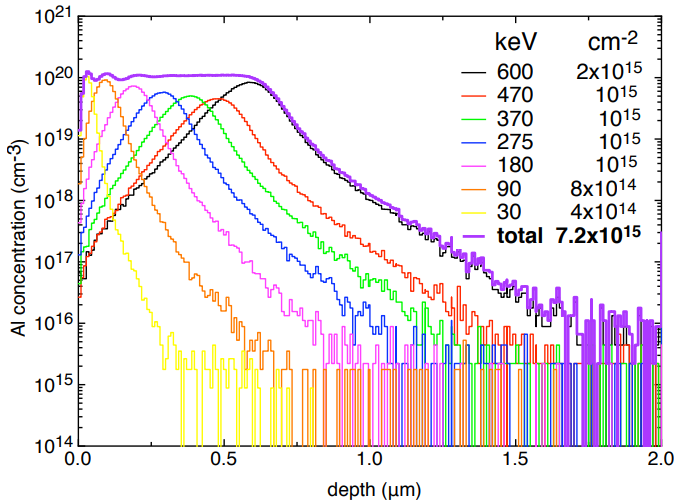
Figure 3 Comparison of multi-step energy ion implantation and wafer surface doping concentration distribution
(Source: G.Lulli, Introduction To Ion Implantation)
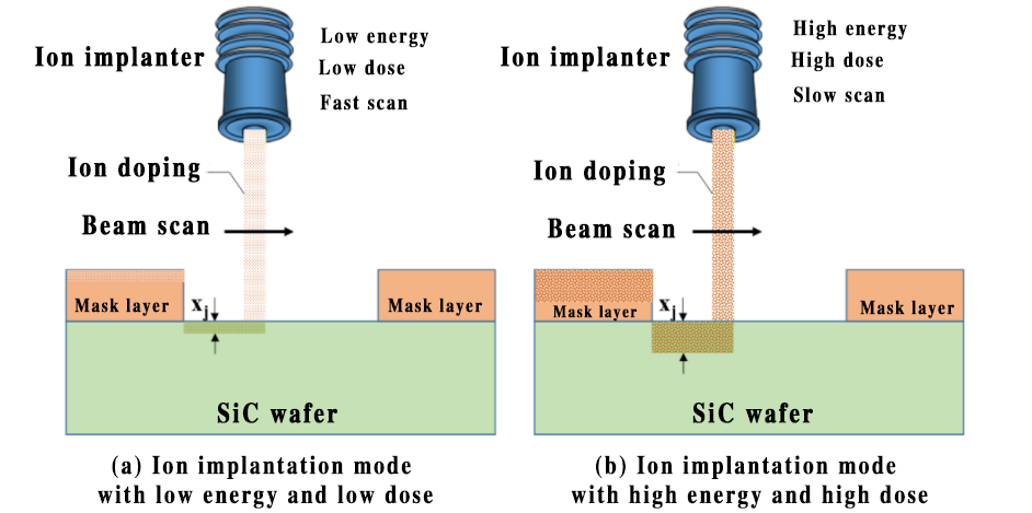
In order to achieve uniform doping concentration in the ion implantation area, engineers usually use multi-step ion implantation to adjust the overall concentration distribution of the implantation area (as shown in Figure 3); in the actual process manufacturing process, by adjusting the implantation energy and implantation dose of the ion implanter, the doping concentration and doping depth of the ion implantation area can be controlled, as shown in Figure 4. (a) and (b); the ion implanter performs uniform ion implantation on the wafer surface by scanning the wafer surface multiple times during operation, as shown in Figure 4. (c).
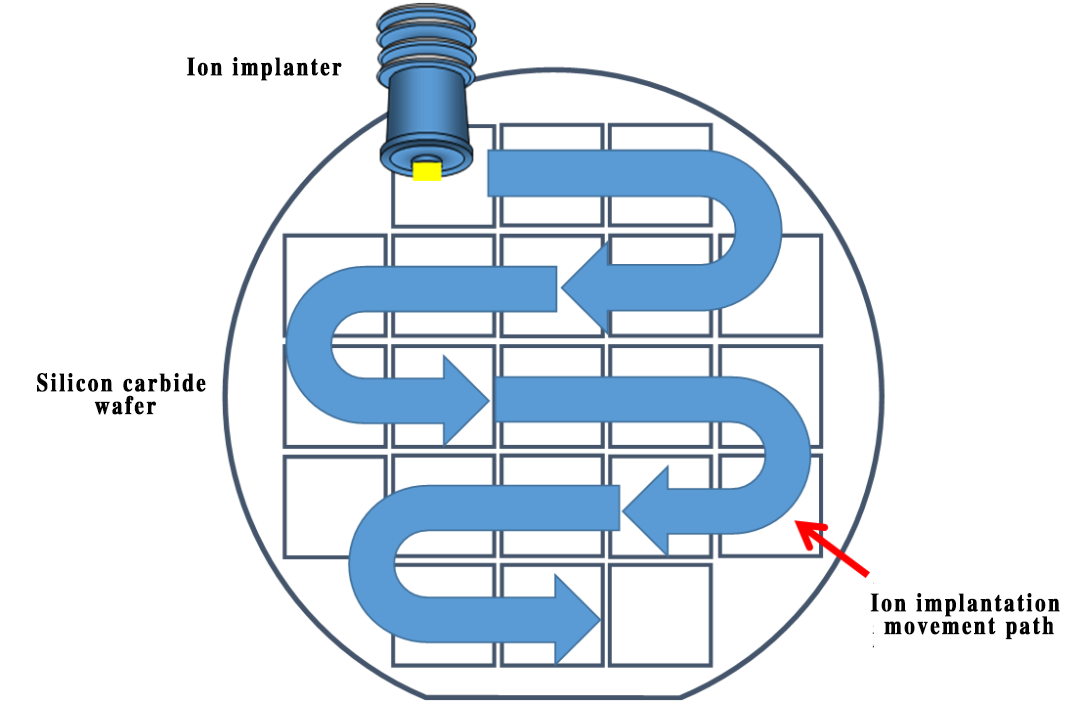
(c) Movement trajectory of the ion implanter during ion implantation
Figure 4 During the ion implantation process, the impurity concentration and depth are controlled by adjusting the ion implantation energy and dose
III
Activation annealing process for silicon carbide ion implantation
The concentration, distribution area, activation rate, defects in the body and on the surface of the ion implantation are the main parameters of the ion implantation process. There are many factors that affect the results of these parameters, including implantation dose, energy, crystal orientation of the material, implantation temperature, annealing temperature, annealing time, environment, etc. Unlike silicon ion implantation doping, it is still difficult to completely ionize the impurities of silicon carbide after ion implantation doping. Taking the aluminum acceptor ionization rate in the neutral region of 4H-SiC as an example, at a doping concentration of 1×1017cm-3, the acceptor ionization rate is only about 15% at room temperature (usually the ionization rate of silicon is approximately 100%). In order to achieve the goal of high activation rate and fewer defects, a high-temperature annealing process will be used after ion implantation to recrystallize the amorphous defects generated during implantation, so that the implanted atoms enter the substitution site and are activated, as shown in Figure 5. At present, people’s understanding of the mechanism of the annealing process is still limited. Control and in-depth understanding of the annealing process is one of the research focuses of ion implantation in the future.
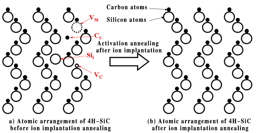
Figure 5 Schematic diagram of the atomic arrangement change on the surface of the silicon carbide ion implantation area before and after ion implantation annealing, where Vsi represents silicon vacancies, VC represents carbon vacancies, Ci represents carbon filling atoms, and Sii represents silicon filling atoms
Ion activation annealing generally includes furnace annealing, rapid annealing and laser annealing. Due to the sublimation of Si atoms in SiC materials, the annealing temperature generally does not exceed 1800℃; the annealing atmosphere is generally carried out in an inert gas or vacuum. Different ions cause different defect centers in SiC and require different annealing temperatures. From most experimental results, it can be concluded that the higher the annealing temperature, the higher the activation rate (as shown in Figure 6).
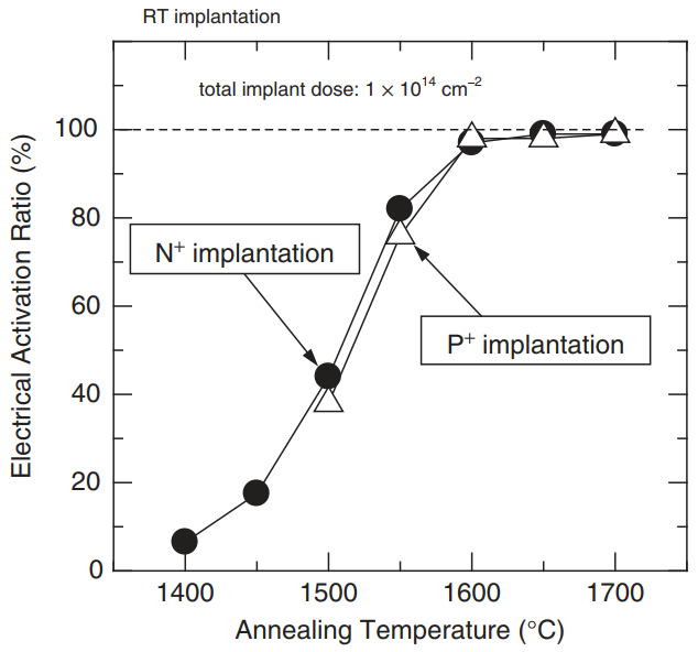
Figure 6 Effect of annealing temperature on the electrical activation rate of nitrogen or phosphorus implantation in SiC (at room temperature)
(Total implantation dose 1×1014cm-2)
(Source: Kimoto, Cooper, Fundamentals of Silicon Carbide Technology: Growth, Characterization, Devices, and Applications)
The commonly used activation annealing process after SiC ion implantation is carried out in an Ar atmosphere at 1600℃~1700℃ to recrystallize the SiC surface and activate the dopant, thereby improving the conductivity of the doped area; before annealing, a layer of carbon film can be coated on the wafer surface for surface protection to reduce surface degradation caused by Si desorption and surface atomic migration, as shown in Figure 7; after annealing, the carbon film can be removed by oxidation or corrosion.
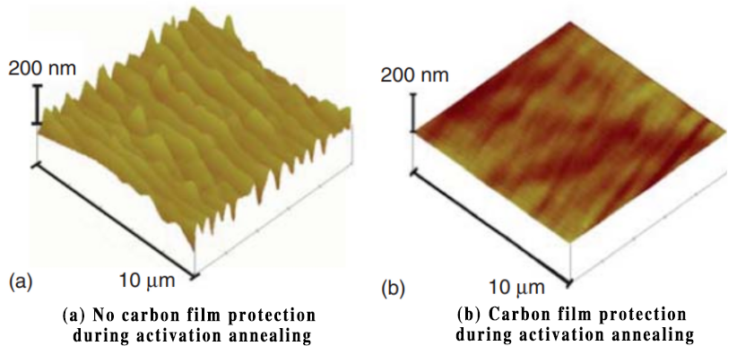
Figure 7 Comparison of surface roughness of 4H-SiC wafers with or without carbon film protection under 1800℃ annealing temperature
(Source: Kimoto, Cooper, Fundamentals of Silicon Carbide Technology: Growth, Characterization, Devices, and Applications)
IV
The impact of SiC ion implantation and activation annealing process
Ion implantation and subsequent activation annealing will inevitably produce defects that reduce device performance: complex point defects, stacking faults (as shown in Figure 8), new dislocations, shallow or deep energy level defects, basal plane dislocation loops and movement of existing dislocations. Since the high-energy ion bombardment process will cause stress to the SiC wafer, the high-temperature and high-energy ion implantation process will increase the wafer warpage. These problems have also become the direction that urgently needs to be optimized and studied in the manufacturing process of SiC ion implantation and annealing.

Figure 8 Schematic diagram of the comparison between normal 4H-SiC lattice arrangement and different stacking faults
(Source: Nicolὸ Piluso 4H-SiC Defects)
V.
Improvement of silicon carbide ion implantation process
(1) A thin oxide film is retained on the surface of the ion implantation area to reduce the degree of implantation damage caused by high-energy ion implantation to the surface of the silicon carbide epitaxial layer, as shown in Figure 9. (a).
(2) Improve the quality of the target disk in the ion implantation equipment, so that the wafer and the target disk fit more closely, the thermal conductivity of the target disk to the wafer is better, and the equipment heats the back of the wafer more uniformly, improving the quality of high-temperature and high-energy ion implantation on silicon carbide wafers, as shown in Figure 9. (b).
(3) Optimize the temperature rise rate and temperature uniformity during the operation of the high-temperature annealing equipment.
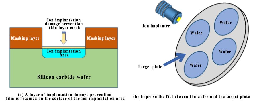
Figure 9 Methods for improving ion implantation process
Post time: Oct-22-2024