Epitaxial layer is a specific single crystal film grown on the wafer by ep·itaxial process, and the substrate wafer and epitaxial film are called epitaxial wafer. By growing the silicon carbide epitaxial layer on the conductive silicon carbide substrate, the silicon carbide homogeneous epitaxial wafer can be further prepared into Schottky diodes, MOSFETs, IGBTs and other power devices, among which 4H-SiC substrate is the most commonly used.
Because of the different manufacturing process of silicon carbide power device and traditional silicon power device, it can not be directly fabricated on silicon carbide single crystal material. Additional high-quality epitaxial materials must be grown on the conductive single crystal substrate, and various devices must be manufactured on the epitaxial layer. Therefore, the quality of the epitaxial layer has great influence on the performance of the device. The improvement of the performance of different power devices also puts forward higher requirements for the thickness of epitaxial layer, doping concentration and defects.
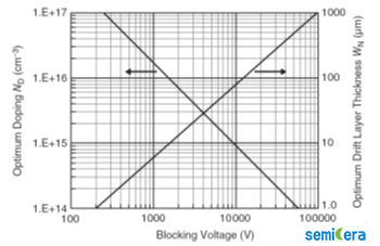
FIG. 1. Relationship between doping concentration and thickness of epitaxial layer of unipolar device and blocking voltage
The preparation methods of SIC epitaxial layer mainly include evaporation growth method, liquid phase epitaxial growth (LPE), molecular beam epitaxial growth (MBE) and chemical vapor deposition (CVD). At present, chemical vapor deposition (CVD) is the main method used for large-scale production in factories.
|
Preparation method |
Advantages of the process |
Disadvantages of the process |
|
Liquid Phase Epitaxial Growth
(LPE)
|
Simple equipment requirements and low-cost growth methods. |
It is difficult to control the surface morphology of the epitaxial layer. The equipment cannot epitaxialize multiple wafers at the same time, limiting mass production. |
|
Molecular Beam Epitaxial Growth (MBE)
|
Different SiC crystal epitaxial layers can be grown at low growth temperatures |
Equipment vacuum requirements are high and costly. Slow growth rate of epitaxial layer |
|
Chemical Vapor Deposition (CVD) |
The most important method for mass production in factories. Growth rate can be precisely controlled when growing thick epitaxial layers. |
SiC epitaxial layers still have various defects that affect device characteristics, so the epitaxial growth process for SiC needs to be continuously optimized.(TaC needed, see Semicera TaC product) |
|
Evaporation growth method
|
Using the same equipment as SiC crystal pulling, the process is slightly different from crystal pulling. Mature equipment, low cost |
Uneven evaporation of SiC makes it difficult to utilize its evaporation to grow high quality epitaxial layers |
FIG. 2. Comparison of main preparation methods of epitaxial layer
On the off-axis {0001} substrate with a certain tilt Angle, as shown in Figure 2(b), the density of the step surface is larger, and the size of the step surface is smaller, and crystal nucleation is not easy to occur on the step surface, but more often occurs at the merging point of the step. In this case, there is only one nucleating key. Therefore, the epitaxial layer can perfectly replicate the stacking order of the substrate, thus eliminating the problem of multi-type coexistence.
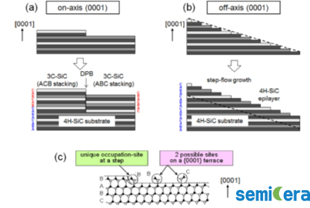
FIG. 3. Physical process diagram of 4H-SiC step control epitaxy method
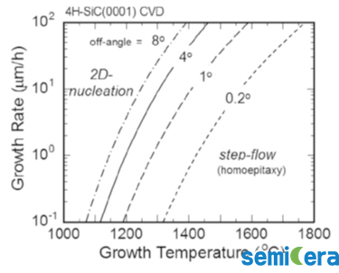
FIG. 4. Critical conditions for CVD growth by 4H-SiC step-controlled epitaxy method
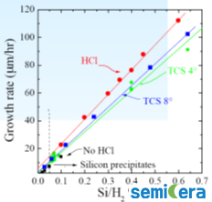
FIG. 5. Comparison of growth rates under different silicon sources in 4H-SiC epitaxy
At present, silicon carbide epitaxy technology is relatively mature in low and medium voltage applications (such as 1200 volt devices). The thickness uniformity, doping concentration uniformity and defect distribution of the epitaxial layer can reach a relatively good level, which can basically meet the needs of middle and low voltage SBD (Schottky diode), MOS (metal oxide semiconductor field effect transistor), JBS (junction diode) and other devices.
However, in the field of high pressure, epitaxial wafers still need to overcome many challenges. For example, for devices that need to withstand 10,000 volts, the thickness of the epitaxial layer needs to be about 100μm. Compared with low-voltage devices, the thickness of the epitaxial layer and the uniformity of the doping concentration are much different, especially the uniformity of the doping concentration. At the same time, the triangle defect in the epitaxial layer will also destroy the overall performance of the device. In high-voltage applications, device types tend to use bipolar devices, which require a high minority lifetime in the epitaxial layer, so the process needs to be optimized to improve the minority lifetime.
At present, the domestic epitaxy is mainly 4 inches and 6 inches, and the proportion of large-size silicon carbide epitaxy is increasing year by year. The size of silicon carbide epitaxial sheet is mainly limited by the size of silicon carbide substrate. At present, the 6-inch silicon carbide substrate has been commercialized, so the silicon carbide epitaxial is gradually transitioning from 4 inches to 6 inches. With the continuous improvement of silicon carbide substrate preparation technology and capacity expansion, the price of silicon carbide substrate is gradually decreasing. In the composition of the epitaxial sheet price, the substrate accounts for more than 50% of the cost, so with the decline of the substrate price, the price of silicon carbide epitaxial sheet is also expected to decrease.
Post time: Jun-03-2024