As we know, in the semiconductor field, single crystal silicon (Si) is the most widely used and largest-volume semiconductor basic material in the world. Currently, more than 90% of semiconductor products are manufactured using silicon-based materials. With the increasing demand for high-power and high-voltage devices in the modern energy field, more stringent requirements have been put forward for key parameters of semiconductor materials such as bandgap width, breakdown electric field strength, electron saturation rate, and thermal conductivity. Under this circumstance, wide bandgap semiconductor materials represented by silicon carbide (SiC) have emerged as the darling of high-power density applications.
As a compound semiconductor, silicon carbide is extremely rare in nature and appears in the form of the mineral moissanite. Currently, almost all silicon carbide sold in the world is artificially synthesized. Silicon carbide has the advantages of high hardness, high thermal conductivity, good thermal stability, and high critical breakdown electric field. It is an ideal material for making high-voltage and high-power semiconductor devices.
So, how are silicon carbide power semiconductor devices manufactured?
What is the difference between the silicon carbide device manufacturing process and the traditional silicon-based manufacturing process? Starting from this issue, “Things about Silicon Carbide Device Manufacturing” will reveal the secrets one by one.
I
Process flow of silicon carbide device manufacturing
The manufacturing process of silicon carbide devices is generally similar to that of silicon-based devices, mainly including photolithography, cleaning, doping, etching, film formation, thinning and other processes. Many power device manufacturers can meet the manufacturing needs of silicon carbide devices by upgrading their production lines based on the silicon-based manufacturing process. However, the special properties of silicon carbide materials determine that some processes in its device manufacturing need to rely on specific equipment for special development to enable silicon carbide devices to withstand high voltage and high current.
II
Introduction to silicon carbide special process modules
The silicon carbide special process modules mainly cover injection doping, gate structure forming, morphology etching, metallization, and thinning processes.
(1) Injection doping: Due to the high carbon-silicon bond energy in silicon carbide, impurity atoms are difficult to diffuse in silicon carbide. When preparing silicon carbide devices, the doping of PN junctions can only be achieved by ion implantation at high temperature.
Doping is usually done with impurity ions such as boron and phosphorus, and the doping depth is usually 0.1μm~3μm. High-energy ion implantation will destroy the lattice structure of the silicon carbide material itself. High-temperature annealing is required to repair the lattice damage caused by ion implantation and control the effect of annealing on surface roughness. The core processes are high-temperature ion implantation and high-temperature annealing.
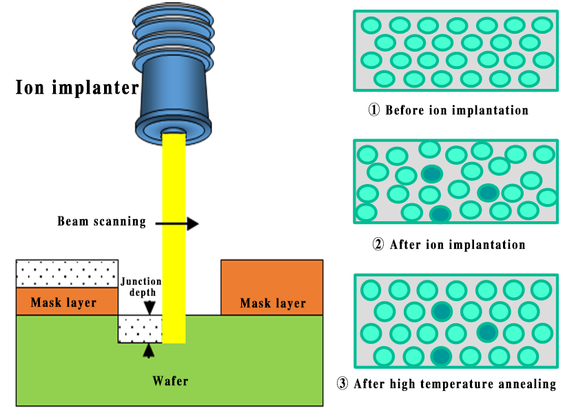
Figure 1 Schematic diagram of ion implantation and high-temperature annealing effects
(2) Gate structure formation: The quality of the SiC/SiO2 interface has a great influence on the channel migration and gate reliability of MOSFET. It is necessary to develop specific gate oxide and post-oxidation annealing processes to compensate for the dangling bonds at the SiC/SiO2 interface with special atoms (such as nitrogen atoms) to meet the performance requirements of high-quality SiC/SiO2 interface and high migration of devices. The core processes are gate oxide high-temperature oxidation, LPCVD, and PECVD.

Figure 2 Schematic diagram of ordinary oxide film deposition and high-temperature oxidation
(3) Morphology etching: Silicon carbide materials are inert in chemical solvents, and precise morphology control can only be achieved through dry etching methods; mask materials, mask etching selection, mixed gas, sidewall control, etching rate, sidewall roughness, etc. need to be developed according to the characteristics of silicon carbide materials. The core processes are thin film deposition, photolithography, dielectric film corrosion, and dry etching processes.
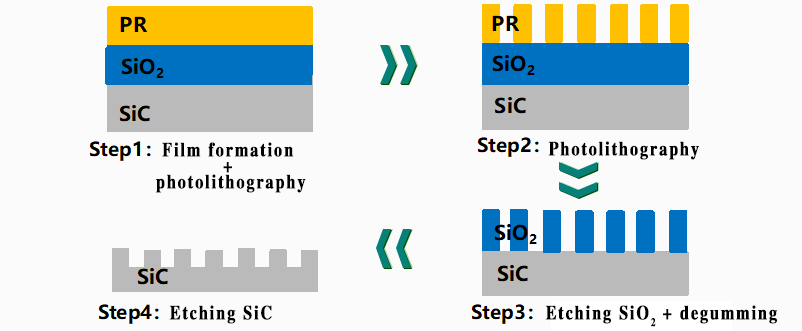
Figure 3 Schematic diagram of silicon carbide etching process
(4) Metallization: The source electrode of the device requires metal to form a good low-resistance ohmic contact with silicon carbide. This not only requires regulating the metal deposition process and controlling the interface state of the metal-semiconductor contact, but also requires high-temperature annealing to reduce the Schottky barrier height and achieve metal-silicon carbide ohmic contact. The core processes are metal magnetron sputtering, electron beam evaporation, and rapid thermal annealing.
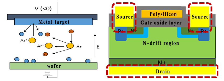
Figure 4 Schematic diagram of magnetron sputtering principle and metallization effect
(5) Thinning process: Silicon carbide material has the characteristics of high hardness, high brittleness and low fracture toughness. Its grinding process is prone to cause brittle fracture of the material, causing damage to the wafer surface and sub-surface. New grinding processes need to be developed to meet the manufacturing needs of silicon carbide devices. The core processes are thinning of grinding discs, film sticking and peeling, etc.
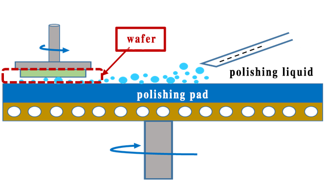
Figure 5 Schematic diagram of wafer grinding/thinning principle
Post time: Oct-22-2024