Wafers are the main raw materials for the production of integrated circuits, discrete semiconductor devices and power devices. More than 90% of integrated circuits are made on high-purity, high-quality wafers.
Wafer preparation equipment refers to the process of making pure polycrystalline silicon materials into silicon single crystal rod materials of a certain diameter and length, and then subjecting the silicon single crystal rod materials to a series of mechanical processing, chemical treatment and other processes.
Equipment that manufactures silicon wafers or epitaxial silicon wafers that meet certain geometric accuracy and surface quality requirements and provides the required silicon substrate for chip manufacturing.
The typical process flow for preparing silicon wafers with a diameter of less than 200 mm is:
Single crystal growth → truncation → outer diameter rolling → slicing → chamfering → grinding → etching → gettering → polishing → cleaning → epitaxy → packaging, etc.
The main process flow for preparing silicon wafers with a diameter of 300 mm is as follows:
Single crystal growth → truncation → outer diameter rolling → slicing → chamfering → surface grinding → etching → edge polishing → double-sided polishing → single-sided polishing → final cleaning → epitaxy/annealing → packaging, etc.
1.Silicon material
Silicon is a semiconductor material because it has 4 valence electrons and is in group IVA of the periodic table along with other elements.
The number of valence electrons in silicon places it right in between a good conductor (1 valence electron) and an insulator (8 valence electrons).
Pure silicon is not found in nature and must be extracted and purified to make it pure enough for manufacturing. It is usually found in silica (silicon oxide or SiO2) and other silicates.
Other forms of SiO2 include glass, colorless crystal, quartz, agate and cat’s eye.
The first material used as a semiconductor was germanium in the 1940s and early 1950s, but it was quickly replaced by silicon.
Silicon was chosen as the main semiconductor material for four main reasons:
Abundance of Silicon Materials: Silicon is the second most abundant element on Earth, accounting for 25% of the Earth’s crust.
The higher melting point of silicon material allows a wider process tolerance: the melting point of silicon at 1412°C is much higher than the melting point of germanium at 937°C. The higher melting point allows silicon to withstand high-temperature processes.
Silicon materials have a wider operating temperature range;
Natural growth of silicon oxide (SiO2): SiO2 is a high-quality, stable electrical insulating material and acts as an excellent chemical barrier to protect silicon from external contamination. Electrical stability is important to avoid leakage between adjacent conductors in integrated circuits. The ability to grow stable thin layers of SiO2 material is fundamental to the manufacture of high-performance metal-oxide semiconductor (MOS-FET) devices. SiO2 has similar mechanical properties to silicon, allowing high-temperature processing without excessive silicon wafer warping.
2.Wafer preparation
Semiconductor wafers are cut from bulk semiconductor materials. This semiconductor material is called a crystal rod, which is grown from a large block of polycrystalline and undoped intrinsic material.
Transforming a polycrystalline block into a large single crystal and giving it the correct crystal orientation and appropriate amount of N-type or P-type doping is called crystal growth.
The most common technologies for producing single crystal silicon ingots for silicon wafer preparation are the Czochralski method and the zone melting method.
2.1 Czochralski method and Czochralski single crystal furnace
The Czochralski (CZ) method, also known as the Czochralski (CZ) method, refers to the process of converting molten semiconductor-grade silicon liquid into solid single-crystal silicon ingots with the correct crystal orientation and doped into N-type or P-type.
Currently, more than 85% of single crystal silicon is grown using the Czochralski method.
A Czochralski single crystal furnace refers to a process equipment that melts high-purity polysilicon materials into liquid by heating in a closed high vacuum or rare gas (or inert gas) protection environment, and then recrystallizes them to form single crystal silicon materials with certain external dimensions.
The working principle of the single crystal furnace is the physical process of polycrystalline silicon material recrystallizing into single crystal silicon material in a liquid state.
The CZ single crystal furnace can be divided into four parts: furnace body, mechanical transmission system, heating and temperature control system, and gas transmission system.
The furnace body includes a furnace cavity, a seed crystal axis, a quartz crucible, a doping spoon, a seed crystal cover, and an observation window.
The furnace cavity is to ensure that the temperature in the furnace is evenly distributed and can dissipate heat well; the seed crystal shaft is used to drive the seed crystal to move up and down and rotate; the impurities that need to be doped are placed in the doping spoon;
The seed crystal cover is to protect the seed crystal from contamination. The mechanical transmission system is mainly used to control the movement of the seed crystal and the crucible.
In order to ensure that the silicon solution is not oxidized, the vacuum degree in the furnace is required to be very high, generally below 5 Torr, and the purity of the added inert gas must be above 99.9999%.
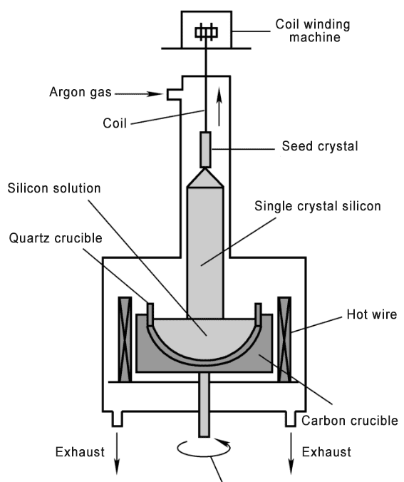
A piece of single crystal silicon with the desired crystal orientation is used as a seed crystal to grow a silicon ingot, and the grown silicon ingot is like a replica of the seed crystal.
The conditions at the interface between the molten silicon and the single crystal silicon seed crystal need to be precisely controlled. These conditions ensure that the thin layer of silicon can accurately replicate the structure of the seed crystal and eventually grow into a large single crystal silicon ingot.
2.2 Zone Melting Method and Zone Melting Single Crystal Furnace
The float zone method (FZ) produces single crystal silicon ingots with very low oxygen content. The float zone method was developed in the 1950s and can produce the purest single crystal silicon to date.
The zone melting single crystal furnace refers to a furnace that uses the principle of zone melting to produce a narrow melting zone in the polycrystalline rod through a high-temperature narrow closed area of the polycrystalline rod furnace body in a high vacuum or rare quartz tube gas protection environment.
A process equipment that moves a polycrystalline rod or a furnace heating body to move the melting zone and gradually crystallize it into a single crystal rod.
The characteristic of preparing single crystal rods by zone melting method is that the purity of polycrystalline rods can be improved in the process of crystallization into single crystal rods, and the doping growth of rod materials is more uniform.
The types of zone melting single crystal furnaces can be divided into two types: floating zone melting single crystal furnaces that rely on surface tension and horizontal zone melting single crystal furnaces. In practical applications, zone melting single crystal furnaces generally adopt floating zone melting.
The zone melting single crystal furnace can prepare high-purity low-oxygen single crystal silicon without the need for a crucible. It is mainly used to prepare high-resistivity (>20kΩ·cm) single crystal silicon and purify zone melting silicon. These products are mainly used in the manufacture of discrete power devices.
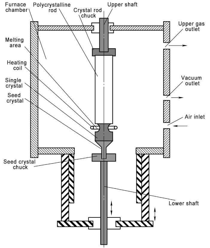
The zone melting single crystal furnace consists of a furnace chamber, an upper shaft and a lower shaft (mechanical transmission part), a crystal rod chuck, a seed crystal chuck, a heating coil (high frequency generator), gas ports (vacuum port, gas inlet, upper gas outlet), etc.
In the furnace chamber structure, cooling water circulation is arranged. The lower end of the upper shaft of the single crystal furnace is a crystal rod chuck, which is used to clamp a polycrystalline rod; the top end of the lower shaft is a seed crystal chuck, which is used to clamp the seed crystal.
A high-frequency power supply is supplied to the heating coil, and a narrow melting zone is formed in the polycrystalline rod starting from the lower end. At the same time, the upper and lower axes rotate and descend, so that the melting zone is crystallized into a single crystal.
The advantages of the zone melting single crystal furnace are that it can not only improve the purity of the prepared single crystal, but also make the rod doping growth more uniform, and the single crystal rod can be purified through multiple processes.
The disadvantages of the zone melting single crystal furnace are high process costs and small diameter of the prepared single crystal. Currently, the maximum diameter of the single crystal that can be prepared is 200mm.
The overall height of the zone melting single crystal furnace equipment is relatively high, and the stroke of the upper and lower axes is relatively long, so longer single crystal rods can be grown.
3. Wafer processing and equipment
The crystal rod needs to go through a series of processes to form a silicon substrate that meets the requirements of semiconductor manufacturing, namely a wafer. The basic process of processing is:
Tumbling, cutting, slicing, wafer annealing, chamfering, grinding, polishing, cleaning and packaging, etc.
3.1 Wafer Annealing
In the process of manufacturing polycrystalline silicon and Czochralski silicon, single crystal silicon contains oxygen. At a certain temperature, the oxygen in the single crystal silicon will donate electrons, and the oxygen will be converted into oxygen donors. These electrons will combine with impurities in the silicon wafer and affect the resistivity of the silicon wafer.
Annealing furnace: refers to a furnace that raises the temperature in the furnace to 1000-1200°C in a hydrogen or argon environment. By keeping warm and cooling, the oxygen near the surface of the polished silicon wafer is volatilized and removed from its surface, causing the oxygen to precipitate and layer.
Process equipment that dissolves micro defects on the surface of silicon wafers, reduces the amount of impurities near the surface of silicon wafers, reduces defects, and forms a relatively clean area on the surface of silicon wafers.
The annealing furnace is also called a high-temperature furnace because of its high temperature. The industry also calls the silicon wafer annealing process gettering.
Silicon wafer annealing furnace is divided into:
-Horizontal annealing furnace;
-Vertical annealing furnace;
-Rapid annealing furnace.
The main difference between a horizontal annealing furnace and a vertical annealing furnace is the layout direction of the reaction chamber.
The reaction chamber of the horizontal annealing furnace is horizontally structured, and a batch of silicon wafers can be loaded into the reaction chamber of the annealing furnace for annealing at the same time. The annealing time is usually 20 to 30 minutes, but the reaction chamber needs a longer heating time to reach the temperature required by the annealing process.
The process of the vertical annealing furnace also adopts the method of simultaneously loading a batch of silicon wafers into the reaction chamber of the annealing furnace for annealing treatment. The reaction chamber has a vertical structure layout, which allows the silicon wafers to be placed in a quartz boat in a horizontal state.
At the same time, since the quartz boat can rotate as a whole in the reaction chamber, the annealing temperature of the reaction chamber is uniform, the temperature distribution on the silicon wafer is uniform, and it has excellent annealing uniformity characteristics. However, the process cost of the vertical annealing furnace is higher than that of the horizontal annealing furnace.
The rapid annealing furnace uses a halogen tungsten lamp to directly heat the silicon wafer, which can achieve rapid heating or cooling in a wide range of 1 to 250°C/s. The heating or cooling rate is faster than that of a traditional annealing furnace. It only takes a few seconds to heat the reaction chamber temperature to above 1100°C.
————————————————————————————————————————————————————
Semicera can provide graphite parts, soft/rigid felt, silicon carbide parts, CVD silicon carbide parts, and SiC/TaC coated parts with full semiconductor process in 30 days.
If you are interested in the above semiconductor products, please do not hesitate to contact us at the first time.
Tel: +86-13373889683
WhatsAPP: +86-15957878134
Email: sales01@semi-cera.com
Post time: Aug-26-2024