1. Introduction
Ion implantation is one of the main processes in integrated circuit manufacturing. It refers to the process of accelerating an ion beam to a certain energy (generally in the range of keV to MeV) and then injecting it into the surface of a solid material to change the physical properties of the surface of the material. In the integrated circuit process, the solid material is usually silicon, and the implanted impurity ions are usually boron ions, phosphorus ions, arsenic ions, indium ions, germanium ions, etc. The implanted ions can change the conductivity of the surface of the solid material or form a PN junction. When the feature size of integrated circuits was reduced to the sub-micron era, the ion implantation process was widely used.
In the integrated circuit manufacturing process, ion implantation is usually used for deep buried layers, reverse doped wells, threshold voltage adjustment, source and drain extension implantation, source and drain implantation, polysilicon gate doping, forming PN junctions and resistors/capacitors, etc. In the process of preparing silicon substrate materials on insulators, the buried oxide layer is mainly formed by high-concentration oxygen ion implantation, or intelligent cutting is achieved by high-concentration hydrogen ion implantation.
Ion implantation is performed by an ion implanter, and its most important process parameters are dose and energy: the dose determines the final concentration, and the energy determines the range (i.e., depth) of the ions. According to different device design requirements, the implantation conditions are divided into high-dose high-energy, medium-dose medium-energy, medium-dose low-energy, or high-dose low-energy. In order to obtain the ideal implantation effect, different implanters should be equipped for different process requirements.
After ion implantation, it is generally necessary to undergo a high-temperature annealing process to repair the lattice damage caused by ion implantation and activate impurity ions. In traditional integrated circuit processes, although the annealing temperature has a great influence on doping, the temperature of the ion implantation process itself is not important. At technology nodes below 14nm, certain ion implantation processes need to be performed in low or high temperature environments to change the effects of lattice damage, etc.
2. ion implantation process
2.1 Basic Principles
Ion implantation is a doping process developed in the 1960s that is superior to traditional diffusion techniques in most aspects.
The main differences between ion implantation doping and traditional diffusion doping are as follows:
(1) The distribution of impurity concentration in the doped region is different. The peak impurity concentration of ion implantation is located inside the crystal, while the peak impurity concentration of diffusion is located on the surface of the crystal. (2) Ion implantation is a process carried out at room temperature or even low temperature, and the production time is short. Diffusion doping requires a longer high-temperature treatment. (3) Ion implantation allows for more flexible and precise selection of implanted elements. (4) Since impurities are affected by thermal diffusion, the waveform formed by ion implantation in the crystal is better than the waveform formed by diffusion in the crystal. (5) Ion implantation usually only uses photoresist as the mask material, but diffusion doping requires the growth or deposition of a film of a certain thickness as a mask. (6) Ion implantation has basically replaced diffusion and become the main doping process in the manufacture of integrated circuits today.
When an incident ion beam with a certain energy bombards a solid target (usually a wafer), the ions and the atoms on the target surface will undergo a variety of interactions, and transfer energy to the target atoms in a certain way to excite or ionize them. The ions can also lose a certain amount of energy through momentum transfer, and finally be scattered by the target atoms or stop in the target material. If the injected ions are heavier, most of the ions will be injected into the solid target. On the contrary, if the injected ions are lighter, many of the injected ions will bounce off the target surface. Basically, these high-energy ions injected into the target will collide with the lattice atoms and electrons in the solid target to varying degrees. Among them, the collision between ions and solid target atoms can be regarded as an elastic collision because they are close in mass.
2.2 Main parameters of ion implantation
Ion implantation is a flexible process that must meet strict chip design and production requirements. Important ion implantation parameters are: dose, range.
Dose (D) refers to the number of ions injected per unit area of the silicon wafer surface, in atoms per square centimeter (or ions per square centimeter). D can be calculated by the following formula:
Where D is the implantation dose (number of ions/unit area); t is the implantation time; I is the beam current; q is the charge carried by the ion (a single charge is 1.6×10¹⁹C[1]); and S is the implantation area.
One of the main reasons why ion implantation has become an important technology in silicon wafer manufacturing is that it can repeatedly implant the same dose of impurities into silicon wafers. The implanter achieves this goal with the help of the positive charge of the ions. When the positive impurity ions form an ion beam, its flow rate is called the ion beam current, which is measured in mA. The range of medium and low currents is 0.1 to 10 mA, and the range of high currents is 10 to 25 mA.
The magnitude of the ion beam current is a key variable in defining the dose. If the current increases, the number of impurity atoms implanted per unit time also increases. High current is conducive to increasing silicon wafer yield (injecting more ions per unit production time), but it also causes uniformity problems.
3. ion implantation equipment
3.1 Basic Structure
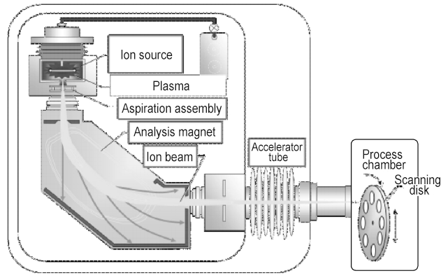
Ion implantation equipment includes 7 basic modules:
① ion source and absorber;
② mass analyzer (i.e. analytical magnet);
③ accelerator tube;
④ scanning disk;
⑤ electrostatic neutralization system;
⑥ process chamber;
⑦ dose control system.
All modules are in a vacuum environment established by the vacuum system. The basic structural diagram of the ion implanter is shown in the figure below.
(1) Ion source:
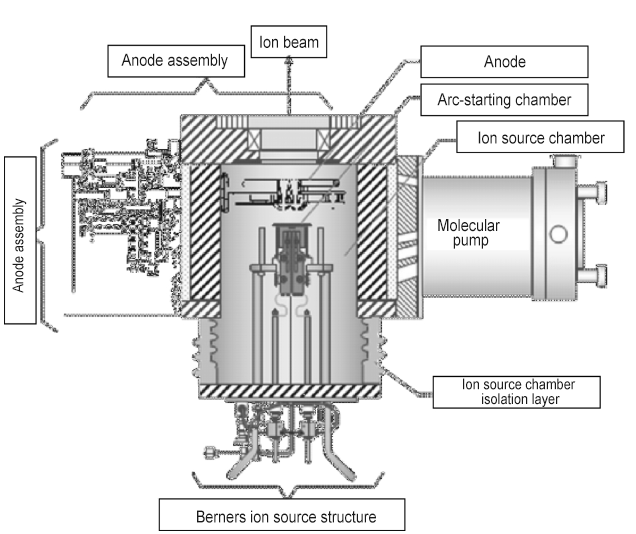
Usually in the same vacuum chamber as the suction electrode. The impurities waiting to be injected must exist in an ion state in order to be controlled and accelerated by the electric field. The most commonly used B+, P+, As+, etc. are obtained by ionizing atoms or molecules.
The impurity sources used are BF3, PH3 and AsH3, etc., and their structures are shown in the figure below. The electrons released by the filament collide with gas atoms to produce ions. Electrons are usually generated by a hot tungsten filament source. For example, the Berners ion source, the cathode filament is installed in an arc chamber with a gas inlet. The inner wall of the arc chamber is the anode.
When the gas source is introduced, a large current passes through the filament, and a voltage of 100 V is applied between the positive and negative electrodes, which will generate high-energy electrons around the filament. Positive ions are generated after the high-energy electrons collide with the source gas molecules.
The external magnet applies a magnetic field parallel to the filament to increase ionization and stabilize the plasma. In the arc chamber, at the other end relative to the filament, there is a negatively charged reflector that reflects the electrons back to improve the generation and efficiency of electrons.
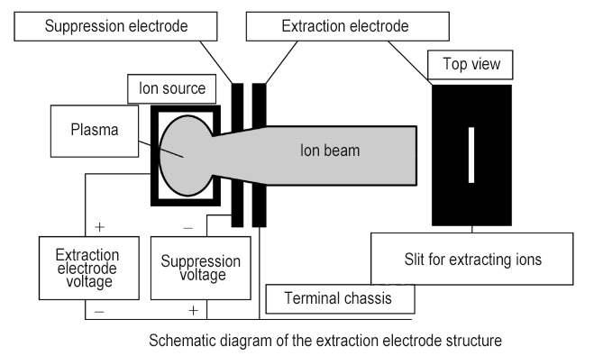
(2) Absorption:
It is used to collect positive ions generated in the arc chamber of the ion source and form them into an ion beam. Since the arc chamber is the anode and the cathode is negatively pressurized on the suction electrode, the electric field generated controls the positive ions, causing them to move toward the suction electrode and be drawn out from the ion slit, as shown in the figure below. The greater the electric field strength, the greater the kinetic energy the ions gain after acceleration. There is also a suppression voltage on the suction electrode to prevent interference from electrons in the plasma. At the same time, the suppression electrode can form ions into an ion beam and focus them into a parallel ion beam stream so that it passes through the implanter.
(3) Mass analyzer:
There may be many kinds of ions generated from the ion source. Under the acceleration of the anode voltage, the ions move at a high speed. Different ions have different atomic mass units and different mass-to-charge ratios.
(4) Accelerator tube:
In order to obtain higher speed, higher energy is required. In addition to the electric field provided by the anode and mass analyzer, an electric field provided in the accelerator tube is also required for acceleration. The accelerator tube consists of a series of electrodes isolated by a dielectric, and the negative voltage on the electrodes increases in sequence through the series connection. The higher the total voltage, the greater the speed obtained by the ions, that is, the greater the energy carried. High energy can allow impurity ions to be injected deep into the silicon wafer to form a deep junction, while low energy can be used to make a shallow junction.
(5) Scanning disk
The focused ion beam is usually very small in diameter. The beam spot diameter of a medium beam current implanter is about 1 cm, and that of a large beam current implanter is about 3 cm. The entire silicon wafer must be covered by scanning. The repeatability of the dose implantation is determined by scanning. Usually, there are four types of implanter scanning systems:
① electrostatic scanning;
② mechanical scanning;
③ hybrid scanning;
④ parallel scanning.
(6) Static electricity neutralization system:
During the implantation process, the ion beam hits the silicon wafer and causes charge to accumulate on the mask surface. The resulting charge accumulation changes the charge balance in the ion beam, making the beam spot larger and the dose distribution uneven. It may even break through the surface oxide layer and cause device failure. Now, the silicon wafer and ion beam are usually placed in a stable high-density plasma environment called a plasma electron shower system, which can control the charging of the silicon wafer. This method extracts electrons from the plasma (usually argon or xenon) in an arc chamber located in the ion beam path and near the silicon wafer. The plasma is filtered and only secondary electrons can reach the surface of the silicon wafer to neutralize the positive charge.
(7) Process cavity:
The injection of ion beams into silicon wafers occurs in the process chamber. The process chamber is an important part of the implanter, including a scanning system, a terminal station with a vacuum lock for loading and unloading silicon wafers, a silicon wafer transfer system, and a computer control system. In addition, there are some devices for monitoring doses and controlling channel effects. If mechanical scanning is used, the terminal station will be relatively large. The vacuum of the process chamber is pumped to the bottom pressure required by the process by a multi-stage mechanical pump, a turbomolecular pump, and a condensation pump, which is generally about 1×10⁻⁶Torr or less.
(8) Dosage control system:
Real-time dose monitoring in an ion implanter is accomplished by measuring the ion beam reaching the silicon wafer. The ion beam current is measured using a sensor called a Faraday cup. In a simple Faraday system, there is a current sensor in the ion beam path that measures the current. However, this presents a problem, as the ion beam reacts with the sensor and produces secondary electrons that will result in erroneous current readings. A Faraday system can suppress secondary electrons using electric or magnetic fields to obtain a true beam current reading. The current measured by the Faraday system is fed into an electronic dose controller, which acts as a current accumulator (which continuously accumulates the measured beam current). The controller is used to relate the total current to the corresponding implantation time and calculate the time required for a certain dose.
3.2 Damage repair
Ion implantation will knock atoms out of the lattice structure and damage the silicon wafer lattice. If the implanted dose is large, the implanted layer will become amorphous. In addition, the implanted ions basically do not occupy the lattice points of silicon, but stay in the lattice gap positions. These interstitial impurities can only be activated after a high-temperature annealing process.
Annealing can heat the implanted silicon wafer to repair lattice defects; it can also move impurity atoms to the lattice points and activate them. The temperature required to repair lattice defects is about 500°C, and the temperature required to activate impurity atoms is about 950°C. The activation of impurities is related to time and temperature: the longer the time and the higher the temperature, the more fully the impurities are activated. There are two basic methods for annealing silicon wafers:
① high-temperature furnace annealing;
② rapid thermal annealing (RTA).
High temperature furnace annealing: High temperature furnace annealing is a traditional annealing method, which uses a high temperature furnace to heat the silicon wafer to 800-1000℃ and keep it for 30 minutes. At this temperature, the silicon atoms move back to the lattice position, and impurity atoms can also replace the silicon atoms and enter the lattice. However, heat treatment at such a temperature and time will lead to the diffusion of impurities, which is something that the modern IC manufacturing industry does not want to see.
Rapid Thermal Annealing: Rapid thermal annealing (RTA) treats silicon wafers with extremely fast temperature rise and short duration at the target temperature (usually 1000°C). Annealing of implanted silicon wafers is usually performed in a rapid thermal processor with Ar or N2. The rapid temperature rise process and short duration can optimize the repair of lattice defects, activation of impurities and inhibition of impurity diffusion. RTA can also reduce transient enhanced diffusion and is the best way to control junction depth in shallow junction implants.
—————————————————————————————————————————————————————————————-
Semicera can provide graphite parts, soft/rigid felt, silicon carbide parts, CVD silicon carbide parts, and SiC/TaC coated parts with in 30 days.
If you are interested in the above semiconductor products, please do not hesitate to contact us at the first time.
Tel: +86-13373889683
WhatsAPP: +86-15957878134
Email: sales01@semi-cera.com
Post time: Aug-31-2024