One Introduction
Etching in the integrated circuit manufacturing process is divided into:
-Wet etching;
-Dry etching.
In the early days, wet etching was widely used, but due to its limitations in line width control and etching directionality, most processes after 3μm use dry etching. Wet etching is only used to remove certain special material layers and clean residues.
Dry etching refers to the process of using gaseous chemical etchants to react with materials on the wafer to etch away the part of the material to be removed and form volatile reaction products, which are then extracted from the reaction chamber. Etchant is usually generated directly or indirectly from the plasma of the etching gas, so dry etching is also called plasma etching.
1.1 Plasma
Plasma is a gas in a weakly ionized state formed by glow discharge of etching gas under the action of an external electromagnetic field (such as generated by a radio frequency power supply). It includes electrons, ions and neutral active particles. Among them, active particles can directly react chemically with the etched material to achieve etching, but this pure chemical reaction usually only occurs in a very small number of materials and is not directional; when the ions have a certain energy, they can be etched by direct physical sputtering, but the etching rate of this pure physical reaction is extremely low and the selectivity is very poor.
Most plasma etching is completed with the participation of active particles and ions at the same time. In this process, ion bombardment has two functions. One is to destroy the atomic bonds on the surface of the etched material, thereby increasing the rate at which neutral particles react with it; the other is to knock off the reaction products deposited on the reaction interface to facilitate the etchant to fully contact the surface of the etched material, so that the etching continues.
The reaction products deposited on the sidewalls of the etched structure cannot be effectively removed by directional ion bombardment, thereby blocking the etching of the sidewalls and forming anisotropic etching.
Second etching process
2.1 Wet Etching and Cleaning
Wet etching is one of the earliest technologies used in integrated circuit manufacturing. Although most wet etching processes have been replaced by anisotropic dry etching due to its isotropic etching, it still plays an important role in cleaning non-critical layers of larger sizes. Especially in the etching of oxide removal residues and epidermal stripping, it is more effective and economical than dry etching.
The objects of wet etching mainly include silicon oxide, silicon nitride, single crystal silicon and polycrystalline silicon. Wet etching of silicon oxide usually uses hydrofluoric acid (HF) as the main chemical carrier. In order to improve selectivity, dilute hydrofluoric acid buffered by ammonium fluoride is used in the process. In order to maintain the stability of the pH value, a small amount of strong acid or other elements can be added. Doped silicon oxide is more easily corroded than pure silicon oxide. Wet chemical stripping is mainly used to remove photoresist and hard mask (silicon nitride). Hot phosphoric acid (H3PO4) is the main chemical liquid used for wet chemical stripping to remove silicon nitride, and has a good selectivity for silicon oxide.
Wet cleaning is similar to wet etching, and mainly removes pollutants on the surface of silicon wafers through chemical reactions, including particles, organic matter, metals and oxides. The mainstream wet cleaning is wet chemical method. Although dry cleaning can replace many wet cleaning methods, there is no method that can completely replace wet cleaning.
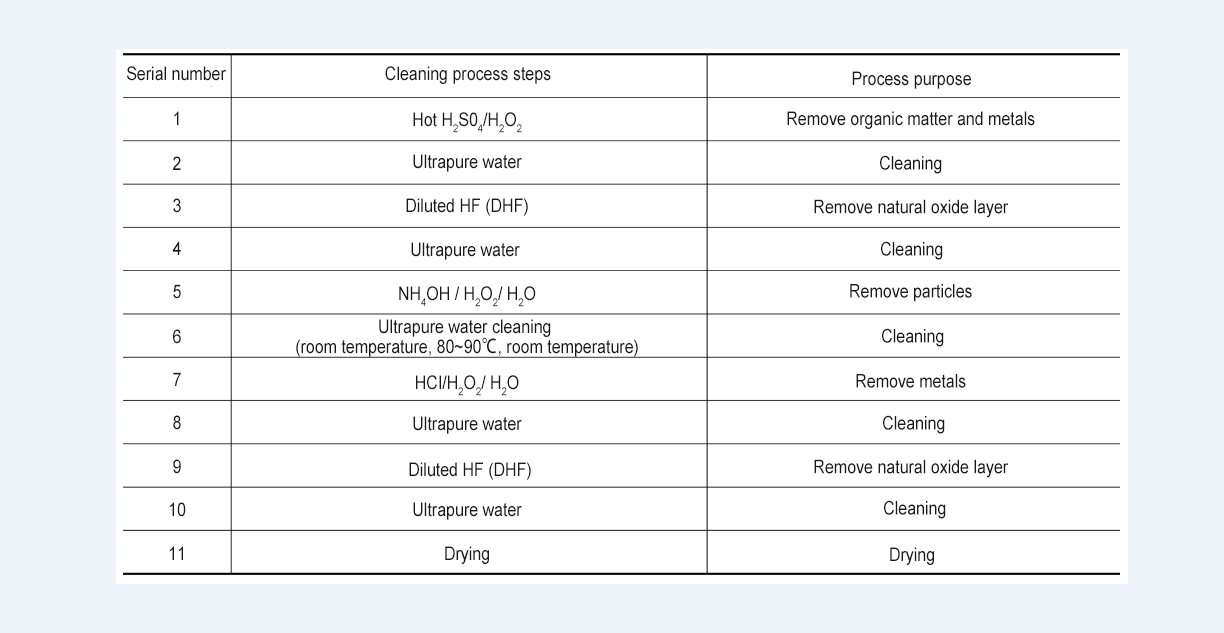
Commonly used chemicals for wet cleaning include sulfuric acid, hydrochloric acid, hydrofluoric acid, phosphoric acid, hydrogen peroxide, ammonium hydroxide, ammonium fluoride, etc. In practical applications, one or more chemicals are mixed with deionized water in a certain proportion as needed to form a cleaning solution, such as SC1, SC2, DHF, BHF, etc.
Cleaning is often used in the process before oxide film deposition, because the preparation of oxide film must be carried out on an absolutely clean silicon wafer surface. The common silicon wafer cleaning process is as follows:
2.2 Dry Etching and Cleaning
2.2.1 Dry Etching
Dry etching in the industry mainly refers to plasma etching, which uses plasma with enhanced activity to etch specific substances. The equipment system in large-scale production processes uses low-temperature non-equilibrium plasma.
Plasma etching mainly uses two discharge modes: capacitive coupled discharge and inductive coupled discharge
In the capacitively coupled discharge mode: plasma is generated and maintained in two parallel plate capacitors by an external radio frequency (RF) power supply. The gas pressure is usually several millitorr to tens of millitorr, and the ionization rate is less than 10-5. In the inductively coupled discharge mode: generally at a lower gas pressure (tens of millitorr), the plasma is generated and maintained by inductively coupled input energy. The ionization rate is usually greater than 10-5, so it is also called high-density plasma. High-density plasma sources can also be obtained through electron cyclotron resonance and cyclotron wave discharge. High-density plasma can optimize the etching rate and selectivity of the etching process while reducing etching damage by independently controlling the ion flow and ion bombardment energy through an external RF or microwave power supply and an RF bias power supply on the substrate.
The dry etching process is as follows: the etching gas is injected into the vacuum reaction chamber, and after the pressure in the reaction chamber is stabilized, the plasma is generated by radio frequency glow discharge; after being impacted by high-speed electrons, it decomposes to produce free radicals, which diffuse to the surface of the substrate and are adsorbed. Under the action of ion bombardment, the adsorbed free radicals react with atoms or molecules on the surface of the substrate to form gaseous byproducts, which are discharged from the reaction chamber. The process is shown in the following figure:
Dry etching processes can be divided into the following four categories:
(1) Physical sputtering etching: It mainly relies on the energetic ions in the plasma to bombard the surface of the etched material. The number of atoms sputtered depends on the energy and angle of the incident particles. When the energy and angle remain unchanged, the sputtering rate of different materials usually differs by only 2 to 3 times, so there is no selectivity. The reaction process is mainly anisotropic.
(2) Chemical etching: Plasma provides gas-phase etching atoms and molecules, which react chemically with the surface of the material to produce volatile gases. This purely chemical reaction has good selectivity and exhibits isotropic characteristics without considering the lattice structure.
For example: Si (solid) + 4F → SiF4 (gaseous), photoresist + O (gaseous) → CO2 (gaseous) + H2O (gaseous)
(3) Ion energy driven etching: Ions are both particles that cause etching and energy-carrying particles. The etching efficiency of such energy-carrying particles is more than one order of magnitude higher than that of simple physical or chemical etching. Among them, the optimization of the physical and chemical parameters of the process is the core of controlling the etching process.
(4) Ion-barrier composite etching: It mainly refers to the generation of a polymer barrier protective layer by composite particles during the etching process. Plasma requires such a protective layer to prevent the etching reaction of the sidewalls during the etching process. For example, adding C to Cl and Cl2 etching can produce a chlorocarbon compound layer during etching to protect the sidewalls from being etched.
2.2.1 Dry cleaning
Dry cleaning mainly refers to plasma cleaning. The ions in the plasma are used to bombard the surface to be cleaned, and the atoms and molecules in the activated state interact with the surface to be cleaned, so as to remove and ash the photoresist. Unlike dry etching, the process parameters of dry cleaning usually do not include directional selectivity, so the process design is relatively simple. In large-scale production processes, fluorine-based gases, oxygen or hydrogen are mainly used as the main body of the reaction plasma. In addition, adding a certain amount of argon plasma can enhance the ion bombardment effect, thereby improving the cleaning efficiency.
In the plasma dry cleaning process, the remote plasma method is usually used. This is because in the cleaning process, it is hoped to reduce the bombardment effect of ions in the plasma to control the damage caused by ion bombardment; and the enhanced reaction of chemical free radicals can improve the cleaning efficiency. Remote plasma can use microwaves to generate a stable and high-density plasma outside the reaction chamber, generating a large number of free radicals that enter the reaction chamber to achieve the reaction required for cleaning. Most of the dry cleaning gas sources in the industry use fluorine-based gases, such as NF3, and more than 99% of NF3 is decomposed in microwave plasma. There is almost no ion bombardment effect in the dry cleaning process, so it is beneficial to protect the silicon wafer from damage and extend the life of the reaction chamber.
Three wet etching and cleaning equipment
3.1 Tank-type wafer cleaning machine
The trough-type wafer cleaning machine is mainly composed of a front-opening wafer transfer box transmission module, a wafer loading/unloading transmission module, an exhaust air intake module, a chemical liquid tank module, a deionized water tank module, a drying tank module and a control module. It can clean multiple boxes of wafers at the same time and can achieve dry-in and dry-out of wafers.
3.2 Trench Wafer Etcher
3.3 Single Wafer Wet Processing Equipment
According to different process purposes, single wafer wet process equipment can be divided into three categories. The first category is single wafer cleaning equipment, whose cleaning targets include particles, organic matter, natural oxide layer, metal impurities and other pollutants; the second category is single wafer scrubbing equipment, whose main process purpose is to remove particles on the surface of the wafer; the third category is single wafer etching equipment, which is mainly used to remove thin films. According to different process purposes, single wafer etching equipment can be divided into two types. The first type is mild etching equipment, which is mainly used to remove surface film damage layers caused by high-energy ion implantation; the second type is sacrificial layer removal equipment, which is mainly used to remove barrier layers after wafer thinning or chemical mechanical polishing.
From the perspective of the overall machine architecture, the basic architecture of all types of single-wafer wet process equipment is similar, generally consisting of six parts: main frame, wafer transfer system, chamber module, chemical liquid supply and transfer module, software system and electronic control module.
3.4 Single Wafer Cleaning Equipment
The single wafer cleaning equipment is designed based on the traditional RCA cleaning method, and its process purpose is to clean particles, organic matter, natural oxide layer, metal impurities and other pollutants. In terms of process application, single wafer cleaning equipment is currently widely used in the front-end and back-end processes of integrated circuit manufacturing, including cleaning before and after film formation, cleaning after plasma etching, cleaning after ion implantation, cleaning after chemical mechanical polishing, and cleaning after metal deposition. Except for the high-temperature phosphoric acid process, single wafer cleaning equipment is basically compatible with all cleaning processes.
3.5 Single Wafer Etching Equipment
The process purpose of single wafer etching equipment is mainly thin film etching. According to the process purpose, it can be divided into two categories, namely, light etching equipment (used to remove the surface film damage layer caused by high-energy ion implantation) and sacrificial layer removal equipment (used to remove the barrier layer after wafer thinning or chemical mechanical polishing). The materials that need to be removed in the process generally include silicon, silicon oxide, silicon nitride and metal film layers.
Four dry etching and cleaning equipment
4.1 Classification of plasma etching equipment
In addition to ion sputtering etching equipment that is close to pure physical reaction and degumming equipment that is close to pure chemical reaction, plasma etching can be roughly divided into two categories according to the different plasma generation and control technologies:
-Capacitively Coupled Plasma (CCP) etching;
-Inductively Coupled Plasma (ICP) etching.
4.1.1 CCP
Capacitively coupled plasma etching is to connect the radio frequency power supply to one or both of the upper and lower electrodes in the reaction chamber, and the plasma between the two plates forms a capacitor in a simplified equivalent circuit.
There are two earliest such technologies:
One is the early plasma etching, which connects the RF power supply to the upper electrode and the lower electrode where the wafer is located is grounded. Because the plasma generated in this way will not form a sufficiently thick ion sheath on the surface of the wafer, the energy of ion bombardment is low, and it is usually used in processes such as silicon etching that use active particles as the main etchant.
The other is the early reactive ion etching (RIE), which connects the RF power supply to the lower electrode where the wafer is located, and grounds the upper electrode with a larger area. This technology can form a thicker ion sheath, which is suitable for dielectric etching processes that require higher ion energy to participate in the reaction. On the basis of early reactive ion etching, a DC magnetic field perpendicular to the RF electric field is added to form ExB drift, which can increase the collision chance of electrons and gas particles, thereby effectively improving the plasma concentration and etching rate. This etching is called magnetic field enhanced reactive ion etching (MERIE).
The above three technologies have a common disadvantage, that is, the plasma concentration and its energy cannot be controlled separately. For example, in order to increase the etching rate, the method of increasing the RF power can be used to increase the plasma concentration, but the increased RF power will inevitably lead to an increase in ion energy, which will cause damage to the devices on the wafer. In the past decade, capacitive coupling technology has adopted a design of multiple RF sources, which are connected to the upper and lower electrodes respectively or both to the lower electrode.
By selecting and matching different RF frequencies, the electrode area, spacing, materials and other key parameters are coordinated with each other, the plasma concentration and ion energy can be decoupled as much as possible.
4.1.2 ICP
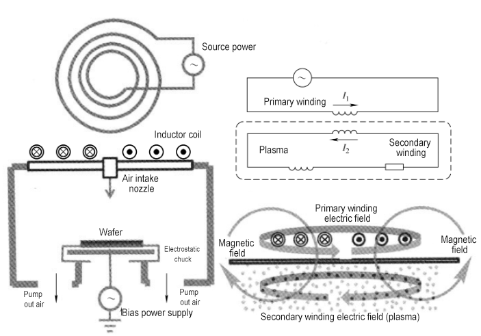
Inductively coupled plasma etching is to place one or more sets of coils connected to a radio frequency power supply on or around the reaction chamber. The alternating magnetic field generated by the radio frequency current in the coil enters the reaction chamber through the dielectric window to accelerate the electrons, thereby generating plasma. In a simplified equivalent circuit (transformer), the coil is the primary winding inductance, and the plasma is the secondary winding inductance.
This coupling method can achieve a plasma concentration that is more than one order of magnitude higher than capacitive coupling at low pressure. In addition, the second RF power supply is connected to the location of the wafer as a bias power supply to provide ion bombardment energy. Therefore, the ion concentration depends on the source power supply of the coil and the ion energy depends on the bias power supply, thereby achieving a more thorough decoupling of concentration and energy.
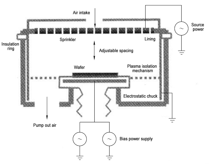
4.2 Plasma Etching Equipment
Almost all etchants in dry etching are directly or indirectly generated from plasma, so dry etching is often called plasma etching. Plasma etching is a type of plasma etching in a broad sense. In the two early flat-plate reactor designs, one is to ground the plate where the wafer is located and the other plate is connected to the RF source; the other is the opposite. In the former design, the area of the grounded plate is usually larger than the area of the plate connected to the RF source, and the gas pressure in the reactor is high. The ion sheath formed on the surface of the wafer is very thin, and the wafer seems to be “immersed” in plasma. Etching is mainly completed by the chemical reaction between the active particles in the plasma and the surface of the etched material. The energy of ion bombardment is very small, and its participation in etching is very low. This design is called plasma etching mode. In another design, because the degree of participation of ion bombardment is relatively large, it is called reactive ion etching mode.
4.3 Reactive Ion Etching Equipment
Reactive ion etching (RIE) refers to an etching process in which active particles and charged ions participate in the process at the same time. Among them, active particles are mainly neutral particles (also known as free radicals), with a high concentration (about 1% to 10% of the gas concentration), which are the main components of the etchant. The products produced by the chemical reaction between them and the etched material are either volatilized and directly extracted from the reaction chamber, or accumulated on the etched surface; while the charged ions are at a lower concentration (10-4 to 10-3 of the gas concentration), and they are accelerated by the electric field of the ion sheath formed on the surface of the wafer to bombard the etched surface. There are two main functions of charged particles. One is to destroy the atomic structure of the etched material, thereby accelerating the rate at which the active particles react with it; the other is to bombard and remove the accumulated reaction products so that the etched material is in full contact with the active particles, so that the etching continues.
Because ions do not directly participate in the etching reaction (or account for a very small proportion, such as physical bombardment removal and direct chemical etching of active ions), strictly speaking, the above etching process should be called ion-assisted etching. The name reactive ion etching is not accurate, but it is still used today. The earliest RIE equipment was put into use in the 1980s. Due to the use of a single RF power supply and a relatively simple reaction chamber design, it has limitations in terms of etching rate, uniformity and selectivity.
4.4 Magnetic Field Enhanced Reactive Ion Etching Equipment
The MERIE (Magnetically Enhanced Reactive Ion Etching) device is an etching device that is constructed by adding a DC magnetic field to a flat-panel RIE device and is intended to increase the etching rate.
MERIE equipment was put into use on a large scale in the 1990s, when single-wafer etching equipment had become the mainstream equipment in the industry. The biggest disadvantage of MERIE equipment is that the spatial distribution inhomogeneity of plasma concentration caused by the magnetic field will lead to current or voltage differences in the integrated circuit device, thereby causing device damage. Since this damage is caused by instantaneous inhomogeneity, the rotation of the magnetic field cannot eliminate it. As the size of integrated circuits continues to shrink, their device damage is increasingly sensitive to plasma inhomogeneity, and the technology of increasing the etching rate by enhancing the magnetic field has gradually been replaced by multi-RF power supply planar reactive ion etching technology, that is, capacitively coupled plasma etching technology.
4.5 Capacitively coupled plasma etching equipment
Capacitively coupled plasma (CCP) etching equipment is a device that generates plasma in a reaction chamber through capacitive coupling by applying a radio frequency (or DC) power supply to the electrode plate and is used for etching. Its etching principle is similar to that of reactive ion etching equipment.
The simplified schematic diagram of the CCP etching equipment is shown below. It generally uses two or three RF sources of different frequencies, and some also use DC power supplies. The frequency of the RF power supply is 800kHz~162MHz, and the commonly used ones are 2MHz, 4MHz, 13MHz, 27MHz, 40MHz and 60MHz. RF power supplies with a frequency of 2MHz or 4MHz are usually called low-frequency RF sources. They are generally connected to the lower electrode where the wafer is located. They are more effective in controlling ion energy, so they are also called bias power supplies; RF power supplies with a frequency above 27MHz are called high-frequency RF sources. They can be connected to either the upper electrode or the lower electrode. They are more effective in controlling plasma concentration, so they are also called source power supplies. The 13MHz RF power supply is in the middle and is generally considered to have both of the above functions but are relatively weaker. Note that although the plasma concentration and energy can be adjusted within a certain range by the power of RF sources of different frequencies (the so-called decoupling effect), due to the characteristics of capacitive coupling, they cannot be adjusted and controlled completely independently.
The energy distribution of ions has a significant impact on the detailed performance of etching and device damage, so the development of technology to optimize ion energy distribution has become one of the key points of advanced etching equipment. Currently, the technologies that have been successfully used in production include multi-RF hybrid drive, DC superposition, RF combined with DC pulse bias, and synchronous pulsed RF output of bias power supply and source power supply.
CCP etching equipment is one of the two most widely used types of plasma etching equipment. It is mainly used in the etching process of dielectric materials, such as gate sidewall and hard mask etching in the front stage of logic chip process, contact hole etching in the middle stage, mosaic and aluminum pad etching in the back stage, as well as etching of deep trenches, deep holes and wiring contact holes in 3D flash memory chip process (taking silicon nitride/silicon oxide structure as an example).
There are two main challenges and improvement directions faced by CCP etching equipment. First, in the application of extremely high ion energy, the etching capability of high aspect ratio structures (such as the hole and groove etching of 3D flash memory requires a ratio higher than 50:1). The current method of increasing the bias power to increase the ion energy has used RF power supplies of up to 10,000 watts. In view of the large amount of heat generated, the cooling and temperature control technology of the reaction chamber needs to be continuously improved. Second, there needs to be a breakthrough in the development of new etching gases to fundamentally solve the problem of etching capability.
4.6 Inductively Coupled Plasma Etching Equipment
Inductively coupled plasma (ICP) etching equipment is a device that couples the energy of a radio frequency power source into a reaction chamber in the form of a magnetic field via an inductor coil, thereby generating plasma for etching. Its etching principle also belongs to the generalized reactive ion etching.
There are two main types of plasma source designs for ICP etching equipment. One is the transformer coupled plasma (TCP) technology developed and produced by Lam Research. Its inductor coil is placed on the dielectric window plane above the reaction chamber. The 13.56MHz RF signal generates an alternating magnetic field in the coil that is perpendicular to the dielectric window and radially diverges with the coil axis as the center.
The magnetic field enters the reaction chamber through the dielectric window, and the alternating magnetic field generates an alternating electric field parallel to the dielectric window in the reaction chamber, thereby achieving the dissociation of the etching gas and generating plasma. Since this principle can be understood as a transformer with an inductor coil as the primary winding and the plasma in the reaction chamber as the secondary winding, ICP etching is named after this.
The main advantage of TCP technology is that the structure is easy to scale up. For example, from a 200mm wafer to a 300mm wafer, TCP can maintain the same etching effect by simply increasing the size of the coil.
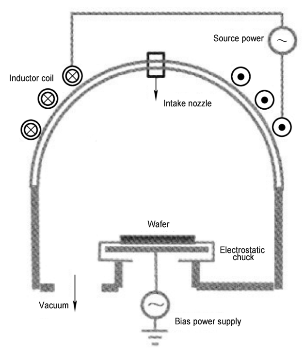
Another plasma source design is the decoupled plasma source (DPS) technology developed and produced by Applied Materials, Inc. of the United States. Its inductor coil is three-dimensionally wound on a hemispherical dielectric window. The principle of generating plasma is similar to the aforementioned TCP technology, but the gas dissociation efficiency is relatively high, which is conducive to obtaining a higher plasma concentration.
Since the efficiency of inductive coupling to generate plasma is higher than that of capacitive coupling, and the plasma is mainly generated in the area close to the dielectric window, its plasma concentration is basically determined by the power of the source power supply connected to the inductor coil, and the ion energy in the ion sheath on the surface of the wafer is basically determined by the power of the bias power supply, so the concentration and energy of the ions can be independently controlled, thereby achieving decoupling.
ICP etching equipment is one of the two most widely used types of plasma etching equipment. It is mainly used for etching of silicon shallow trenches, germanium (Ge), polysilicon gate structures, metal gate structures, strained silicon (Strained-Si), metal wires, metal pads (Pads), mosaic etching metal hard masks and multiple processes in multiple imaging technology.
In addition, with the rise of three-dimensional integrated circuits, CMOS image sensors and micro-electro-mechanical systems (MEMS), as well as the rapid increase in the application of through silicon vias (TSV), large-size oblique holes and deep silicon etching with different morphologies, many manufacturers have launched etching equipment developed specifically for these applications. Its characteristics are large etching depth (tens or even hundreds of microns), so it mostly works under high gas flow, high pressure and high power conditions.
—————————————————————————————————————————————————————————————-
Semicera can provide graphite parts, soft/rigid felt, silicon carbide parts, CVD silicon carbide parts, and SiC/TaC coated parts with in 30 days.
If you are interested in the above semiconductor products, please do not hesitate to contact us at the first time.
Tel: +86-13373889683
WhatsAPP: +86-15957878134
Email: sales01@semi-cera.com
Post time: Aug-31-2024