One Overview
In the integrated circuit manufacturing process, photolithography is the core process that determines the integration level of integrated circuits. The function of this process is to faithfully transmit and transfer the circuit graphic information from the mask (also called the mask) to the semiconductor material substrate.
The basic principle of the photolithography process is to utilize the photochemical reaction of the photoresist coated on the surface of the substrate to record the circuit pattern on the mask, thereby achieving the purpose of transferring the integrated circuit pattern from the design to the substrate.
The basic process of photolithography
First, photoresist is applied on the substrate surface using a coating machine;
Then, a photolithography machine is used to expose the substrate coated with photoresist, and the photochemical reaction mechanism is used to record the mask pattern information transmitted by the photolithography machine, completing the fidelity transmission, transfer and replication of the mask pattern to the substrate;
Finally, a developer is used to develop the exposed substrate to remove (or retain) the photoresist that undergoes a photochemical reaction after exposure.
Second photolithography process
In order to transfer the designed circuit pattern on the mask to the silicon wafer, the transfer must first be achieved through an exposure process, and then the silicon pattern must be obtained through an etching process.
Since the illumination of the photolithography process area uses a yellow light source to which photosensitive materials are insensitive, it is also called the yellow light area.
Photolithography was first used in the printing industry and was the main technology for early PCB manufacturing. Since the 1950s, photolithography has gradually become the mainstream technology for pattern transfer in IC manufacturing.
The key indicators of lithography process include resolution, sensitivity, overlay accuracy, defect rate, etc.
The most critical material in the photolithography process is the photoresist, which is a photosensitive material. Since the sensitivity of the photoresist depends on the wavelength of the light source, different photoresist materials are required for photolithography processes such as g/i line, 248nm KrF, and 193nm ArF.
The main process of a typical photolithography process includes five steps
:
-Base film preparation;
-Apply photoresist and soft bake;
-Alignment, exposure and post-exposure baking;
-Develop hard film;
-Development detection.
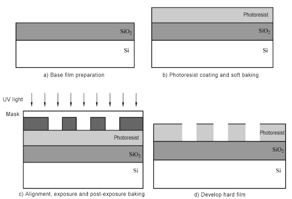
(1) Base film preparation: mainly cleaning and dehydration. Because any contaminants will weaken the adhesion between the photoresist and the wafer, thorough cleaning can improve the adhesion between the wafer and the photoresist.
(2) Photoresist coating: This is achieved by rotating the silicon wafer. Different photoresists require different coating process parameters, including rotation speed, photoresist thickness, and temperature.
Soft baking: Baking can improve the adhesion between the photoresist and the silicon wafer, as well as the uniformity of the photoresist thickness, which is beneficial for the precise control of the geometric dimensions of the subsequent etching process.
(3) Alignment and exposure: Alignment and exposure are the most important steps in the photolithography process. They refer to aligning the mask pattern with the existing pattern on the wafer (or the front layer pattern), and then irradiating it with specific light. The light energy activates the photosensitive components in the photoresist, thereby transferring the mask pattern to the photoresist.
The equipment used for alignment and exposure is a photolithography machine, which is the most expensive single piece of process equipment in the entire integrated circuit manufacturing process. The technical level of the photolithography machine represents the level of advancement of the entire production line.
Post-exposure baking: refers to a short baking process after exposure, which has a different effect than in deep ultraviolet photoresists and conventional i-line photoresists.
For deep ultraviolet photoresist, post-exposure baking removes the protective components in the photoresist, allowing the photoresist to dissolve in the developer, so post-exposure baking is necessary;
For conventional i-line photoresists, post-exposure baking can improve the adhesion of the photoresist and reduce standing waves (standing waves will have an adverse effect on the edge morphology of the photoresist).
(4) Developing the hard film: using developer to dissolve the soluble part of the photoresist (positive photoresist) after exposure, and accurately display the mask pattern with the photoresist pattern.
The key parameters of the development process include development temperature and time, developer dosage and concentration, cleaning, etc. By adjusting the relevant parameters in the development, the difference in dissolution rate between the exposed and unexposed parts of the photoresist can be increased, thereby obtaining the desired development effect.
Hardening is also known as hardening baking, which is the process of removing the remaining solvent, developer, water and other unnecessary residual components in the developed photoresist by heating and evaporating them, so as to improve the adhesion of the photoresist to the silicon substrate and the etching resistance of the photoresist.
The temperature of the hardening process varies depending on the different photoresists and the hardening methods. The premise is that the photoresist pattern does not deform and the photoresist should be made hard enough.
(5) Development inspection: This is to check for defects in the photoresist pattern after development. Usually, image recognition technology is used to automatically scan the chip pattern after development and compare it with the pre-stored defect-free standard pattern. If any difference is found, it is considered to be defective.
If the number of defects exceeds a certain value, the silicon wafer is judged to have failed the development test and may be scrapped or reworked as appropriate.
In the integrated circuit manufacturing process, most processes are irreversible, and photolithography is one of the very few processes that can be reworked.
Three photomasks and photoresist materials
3.1 Photomask
A photomask, also known as a photolithography mask, is a master used in the photolithography process of integrated circuit wafer manufacturing.
The photomask manufacturing process is to convert the original layout data required for wafer manufacturing designed by integrated circuit design engineers into a data format that can be recognized by laser pattern generators or electron beam exposure equipment through mask data processing, so that it can be exposed by the above equipment on the photomask substrate material coated with photosensitive material; then it is processed through a series of processes such as development and etching to fix the pattern on the substrate material; finally, it is inspected, repaired, cleaned, and film-laminated to form a mask product and delivered to the integrated circuit manufacturer for use.
3.2 Photoresist
Photoresist, also known as photoresist, is a photosensitive material. The photosensitive components in it will undergo chemical changes under the irradiation of light, thereby causing changes in the dissolution rate. Its main function is to transfer the pattern on the mask to a substrate such as a wafer.
Working principle of photoresist: First, the photoresist is coated on the substrate and pre-baked to remove the solvent;
Secondly, the mask is exposed to light, causing the photosensitive components in the exposed part to undergo a chemical reaction;
Then, a post-exposure bake is performed;
Finally, the photoresist is partially dissolved through development (for positive photoresist, the exposed area is dissolved; for negative photoresist, the unexposed area is dissolved), thereby realizing the transfer of the integrated circuit pattern from the mask to the substrate.
The components of photoresist mainly include film-forming resin, photosensitive component, trace additives and solvent.
Among them, the film-forming resin is used to provide mechanical properties and etching resistance; the photosensitive component undergoes chemical changes under light, causing changes in the dissolution rate;
Trace additives include dyes, viscosity enhancers, etc., which are used to improve the performance of photoresist; solvents are used to dissolve the components and mix them evenly.
The photoresists currently in wide use can be divided into traditional photoresists and chemically amplified photoresists according to the photochemical reaction mechanism, and can also be divided into ultraviolet, deep ultraviolet, extreme ultraviolet, electron beam, ion beam and X-ray photoresists according to the photosensitivity wavelength.
Four photolithography equipment
Photolithography technology has gone through the development process of contact/proximity lithography, optical projection lithography, step-and-repeat lithography, scanning lithography, immersion lithography, and EUV lithography.
4.1 Contact/Proximity Lithography Machine
Contact lithography technology appeared in the 1960s and was widely used in the 1970s. It was the main lithography method in the era of small-scale integrated circuits and was mainly used to produce integrated circuits with feature sizes greater than 5μm.
In a contact/proximity lithography machine, the wafer is usually placed on a manually controlled horizontal position and rotating worktable. The operator uses a discrete field microscope to simultaneously observe the position of the mask and wafer, and manually controls the position of the worktable to align the mask and wafer. After the wafer and mask are aligned, the two will be pressed together so that the mask is in direct contact with the photoresist on the surface of the wafer.
After removing the microscope objective, the pressed wafer and mask are moved to the exposure table for exposure. The light emitted by the mercury lamp is collimated and parallel to the mask through a lens. Since the mask is in direct contact with the photoresist layer on the wafer, the mask pattern is transferred to the photoresist layer at a ratio of 1:1 after exposure.
Contact lithography equipment is the simplest and most economical optical lithography equipment, and can achieve exposure of sub-micron feature size graphics, so it is still used in small-batch product manufacturing and laboratory research. In large-scale integrated circuit production, proximity lithography technology was introduced to avoid the increase in lithography costs caused by direct contact between the mask and the wafer.
Proximity lithography was widely used in the 1970s during the era of small-scale integrated circuits and the early era of medium-scale integrated circuits. Unlike contact lithography, the mask in proximity lithography is not in direct contact with the photoresist on the wafer, but a gap filled with nitrogen is left. The mask floats on the nitrogen, and the size of the gap between the mask and the wafer is determined by the nitrogen pressure.
Since there is no direct contact between the wafer and the mask in proximity lithography, the defects introduced during the lithography process are reduced, thereby reducing the loss of the mask and improving the wafer yield. In proximity lithography, the gap between the wafer and the mask puts the wafer in the Fresnel diffraction region. The presence of diffraction limits the further improvement of the resolution of proximity lithography equipment, so this technology is mainly suitable for the production of integrated circuits with feature sizes above 3μm.
4.2 Stepper and Repeater
The stepper is one of the most important equipment in the history of wafer lithography, which has promoted the sub-micron lithography process into mass production. The stepper uses a typical static exposure field of 22mm × 22mm and an optical projection lens with a reduction ratio of 5:1 or 4:1 to transfer the pattern on the mask to the wafer.
The step-and-repeat lithography machine is generally composed of an exposure subsystem, a workpiece stage subsystem, a mask stage subsystem, a focus/leveling subsystem, an alignment subsystem, a main frame subsystem, a wafer transfer subsystem, a mask transfer subsystem, an electronic subsystem, and a software subsystem.
The typical working process of a step-and-repeat lithography machine is as follows:
First, the wafer coated with photoresist is transferred to the workpiece table by using the wafer transfer subsystem, and the mask to be exposed is transferred to the mask table by using the mask transfer subsystem;
Then, the system uses the focusing/leveling subsystem to perform multi-point height measurement on the wafer on the workpiece stage to obtain information such as the height and tilt angle of the surface of the wafer to be exposed, so that the exposure area of the wafer can always be controlled within the focal depth of the projection objective during the exposure process;Subsequently, the system uses the alignment subsystem to align the mask and wafer so that during the exposure process the position accuracy of the mask image and wafer pattern transfer is always within the overlay requirements.
Finally, the step-and-exposure action of the entire wafer surface is completed according to the prescribed path to realize the pattern transfer function.
The subsequent stepper and scanner lithography machine is based on the above basic working process, improving stepping → exposure to scanning → exposure, and focusing/leveling → alignment → exposure on the dual-stage model to measurement (focusing/leveling → alignment) and scanning exposure in parallel.
Compared with the step-and-scan lithography machine, the step-and-repeat lithography machine does not need to achieve synchronous reverse scanning of the mask and wafer, and does not require a scanning mask table and a synchronous scanning control system. Therefore, the structure is relatively simple, the cost is relatively low, and the operation is reliable.
After IC technology entered 0.25μm, the application of step-and-repeat lithography began to decline due to the advantages of step-and-scan lithography in scanning exposure field size and exposure uniformity. Currently, the latest step-and-repeat lithography provided by Nikon has a static exposure field of view as large as that of the step-and-scan lithography, and can process more than 200 wafers per hour, with extremely high production efficiency. This type of lithography machine is currently mainly used for the manufacture of non-critical IC layers.
4.3 Stepper Scanner
The application of step-and-scan lithography began in the 1990s. By configuring different exposure light sources, step-and-scan technology can support different process technology nodes, from 365nm, 248nm, 193nm immersion to EUV lithography. Unlike step-and-repeat lithography, the single-field exposure of step-and-scan lithography adopts dynamic scanning, that is, the mask plate completes the scanning movement synchronously relative to the wafer; after the current field exposure is completed, the wafer is carried by the workpiece stage and stepped to the next scanning field position, and repeated exposure continues; repeat the step-and-scan exposure multiple times until all fields of the entire wafer are exposed.
By configuring different types of light sources (such as i-line, KrF, ArF), the stepper-scanner can support almost all technology nodes of the semiconductor front-end process. Typical silicon-based CMOS processes have adopted stepper-scanners in large quantities since the 0.18μm node; the extreme ultraviolet (EUV) lithography machines currently used in process nodes below 7nm also use stepper-scanning. After partial adaptive modification, the stepper-scanner can also support the research and development and production of many non-silicon-based processes such as MEMS, power devices, and RF devices.
The main manufacturers of step-and-scan projection lithography machines include ASML (Netherlands), Nikon (Japan), Canon (Japan) and SMEE (China). ASML launched the TWINSCAN series of step-and-scan lithography machines in 2001. It adopts a dual-stage system architecture, which can effectively improve the output rate of the equipment and has become the most widely used high-end lithography machine.
4.4 Immersion Lithography
It can be seen from the Rayleigh formula that, when the exposure wavelength remains unchanged, an effective way to further improve the imaging resolution is to increase the numerical aperture of the imaging system. For imaging resolutions below 45nm and higher, the ArF dry exposure method can no longer meet the requirements (because it supports a maximum imaging resolution of 65nm), so it is necessary to introduce an immersion lithography method. In traditional lithography technology, the medium between the lens and the photoresist is air, while immersion lithography technology replaces the air medium with liquid (usually ultrapure water with a refractive index of 1.44).
In fact, immersion lithography technology uses the shortening of the wavelength of the light source after light passes through the liquid medium to improve the resolution, and the shortening ratio is the refractive index of the liquid medium. Although the immersion lithography machine is a type of step-and-scan lithography machine, and its equipment system solution has not changed, it is a modification and expansion of the ArF step-and-scan lithography machine due to the introduction of key technologies related to immersion.
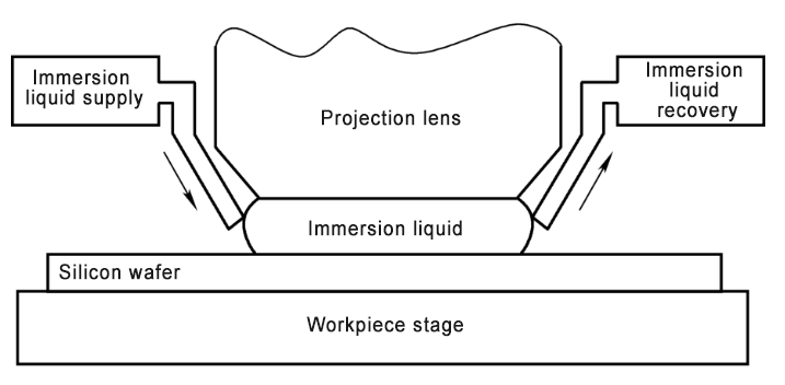
The advantage of immersion lithography is that, due to the increase in the numerical aperture of the system, the imaging resolution capability of the stepper-scanner lithography machine is improved, which can meet the process requirements of imaging resolution below 45nm.
Since the immersion lithography machine still uses ArF light source, the continuity of the process is guaranteed, saving the R&D cost of light source, equipment and process. On this basis, combined with multiple graphics and computational lithography technology, the immersion lithography machine can be used at process nodes of 22nm and below. Before the EUV lithography machine was officially put into mass production, the immersion lithography machine had been widely used and could meet the process requirements of the 7nm node. However, due to the introduction of immersion liquid, the engineering difficulty of the equipment itself has increased significantly.
Its key technologies include immersion liquid supply and recovery technology, immersion liquid field maintenance technology, immersion lithography pollution and defect control technology, development and maintenance of ultra-large numerical aperture immersion projection lenses, and imaging quality detection technology under immersion conditions.
Currently, commercial ArFi step-and-scan lithography machines are mainly provided by two companies, namely ASML of the Netherlands and Nikon of Japan. Among them, the price of a single ASML NXT1980 Di is about 80 million euros.
4.5 Extreme Ultraviolet Lithography Machine
In order to improve the resolution of photolithography, the exposure wavelength is further shortened after the excimer light source is adopted, and extreme ultraviolet light with a wavelength of 10 to 14 nm is introduced as the exposure light source. The wavelength of extreme ultraviolet light is extremely short, and the reflective optical system that can be used is usually composed of multilayer film reflectors such as Mo/Si or Mo/Be.
Among them, the theoretical maximum reflectivity of Mo/Si multilayer film in the wavelength range of 13.0 to 13.5nm is about 70%, and the theoretical maximum reflectivity of Mo/Be multilayer film at a shorter wavelength of 11.1nm is about 80%. Although the reflectivity of Mo/Be multilayer film reflectors is higher, Be is highly toxic, so research on such materials was abandoned when developing EUV lithography technology.The current EUV lithography technology uses Mo/Si multilayer film, and its exposure wavelength is also determined to be 13.5nm.
The mainstream extreme ultraviolet light source uses laser-produced plasma (LPP) technology, which uses high-intensity lasers to excite hot-melt Sn plasma to emit light. For a long time, the power and availability of the light source have been the bottlenecks restricting the efficiency of EUV lithography machines. Through the master oscillator power amplifier, predictive plasma (PP) technology and in-situ collection mirror cleaning technology, the power and stability of EUV light sources have been greatly improved.
The EUV lithography machine is mainly composed of subsystems such as light source, lighting, objective lens, workpiece stage, mask stage, wafer alignment, focusing/leveling, mask transmission, wafer transmission, and vacuum frame. After passing through the illumination system composed of multi-layer coated reflectors, the extreme ultraviolet light is irradiated on the reflective mask. The light reflected by the mask enters the optical total reflection imaging system composed of a series of reflectors, and finally the reflected image of the mask is projected on the surface of the wafer in a vacuum environment.
The exposure field of view and imaging field of view of the EUV lithography machine are both arc-shaped, and a step-by-step scanning method is used to achieve full wafer exposure to improve the output rate. ASML’s most advanced NXE series EUV lithography machine uses an exposure light source with a wavelength of 13.5nm, a reflective mask (6° oblique incidence), a 4x reduction reflective projection objective system with a 6-mirror structure (NA=0.33), a scanning field of view of 26mm × 33mm, and a vacuum exposure environment.
Compared with immersion lithography machines, the single exposure resolution of EUV lithography machines using extreme ultraviolet light sources has been greatly improved, which can effectively avoid the complex process required for multiple photolithography to form high-resolution graphics. At present, the single exposure resolution of the NXE 3400B lithography machine with a numerical aperture of 0.33 reaches 13nm, and the output rate reaches 125 pieces/h.
In order to meet the needs of further extension of Moore’s Law, in the future, EUV lithography machines with a numerical aperture of 0.5 will adopt a projection objective system with central light blocking, using an asymmetric magnification of 0.25 times/0.125 times, and the scanning exposure field of view will be reduced from 26m × 33mm to 26mm × 16.5mm, and the single exposure resolution can reach below 8nm.
—————————————————————————————————————————————————————————————
Semicera can provide graphite parts, soft/rigid felt, silicon carbide parts, CVD silicon carbide parts, and SiC/TaC coated parts with full semiconductor process in 30 days.
If you are interested in the above semiconductor products, please do not hesitate to contact us at the first time.
Tel: +86-13373889683
WhatsAPP: +86-15957878134
Email: sales01@semi-cera.com
Post time: Aug-31-2024