1.About Integrated Circuits
1.1 The concept and birth of integrated circuits
Integrated Circuit (IC): refers to a device that combines active devices such as transistors and diodes with passive components such as resistors and capacitors through a series of specific processing techniques.
A circuit or system that is “integrated” on a semiconductor (such as silicon or compounds such as gallium arsenide) wafer according to certain circuit interconnections and then packaged in a shell to perform specific functions.
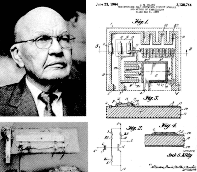
In 1958, Jack Kilby, who was responsible for the miniaturization of electronic equipment at Texas Instruments (TI), proposed the idea of integrated circuits:
“Since all components such as capacitors, resistors, transistors, etc. can be made from one material, I thought it would be possible to make them on a piece of semiconductor material and then interconnect them to form a complete circuit.”
On September 12 and September 19, 1958, Kilby completed the manufacture and demonstration of the phase-shift oscillator and trigger, respectively, marking the birth of the integrated circuit.
In 2000, Kilby was awarded the Nobel Prize in Physics. The Nobel Prize Committee once commented that Kilby “laid the foundation for modern information technology.”
The picture below shows Kilby and his integrated circuit patent:
1.2 Development of semiconductor manufacturing technology
The following figure shows the development stages of semiconductor manufacturing technology: 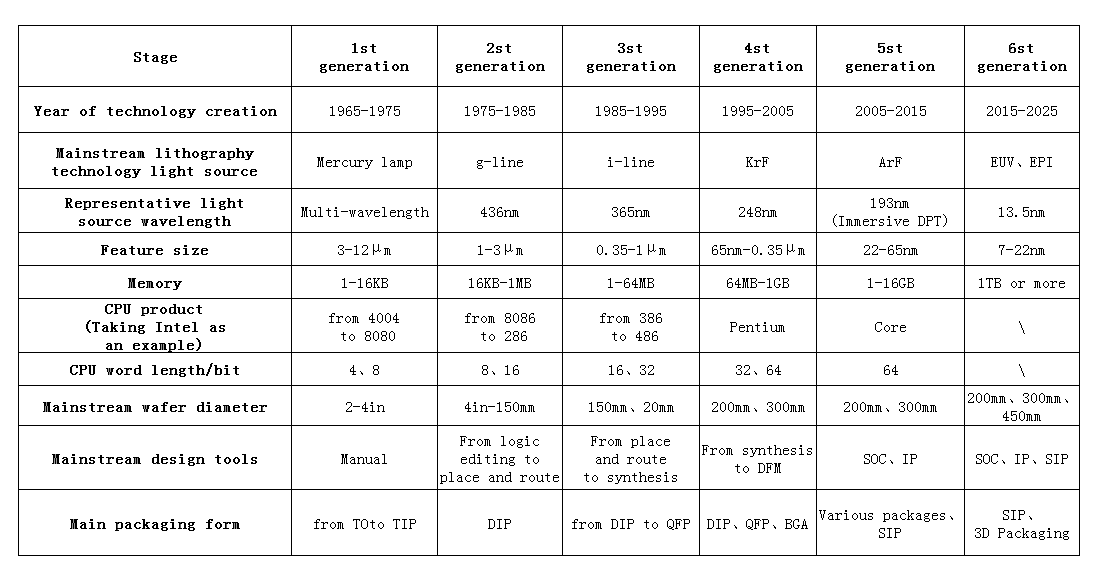
1.3 Integrated Circuit Industry Chain
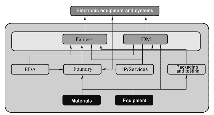
The composition of the semiconductor industry chain (mainly integrated circuits, including discrete devices) is shown in the figure above:
- Fabless: A company that designs products without a production line.
- IDM: Integrated Device Manufacturer, integrated device manufacturer;
- IP: Circuit module manufacturer;
- EDA: Electronic Design Automatic, electronic design automation, the company mainly provides design tools;
- Foundry; Wafer foundry, providing chip manufacturing services;
- Packaging and testing foundry companies: mainly serving Fabless and IDM;
- Materials and special equipment companies: mainly provide the necessary materials and equipment for chip manufacturing companies.
The main products produced using semiconductor technology are integrated circuits and discrete semiconductor devices.
The main products of integrated circuits include:
- Application Specific Standard Parts (ASSP);
- Microprocessor Unit (MPU);
- Memory
- Application Specific Integrated Circuit (ASIC);
- Analog Circuit;
- General logic circuit (Logical Circuit).
The main products of semiconductor discrete devices include:
- Diode;
- Transistor;
- Power Device;
- High-Voltage Device;
- Microwave Device;
- Optoelectronics;
- Sensor device (Sensor).
2. Integrated Circuit Manufacturing Process
2.1 Chip Manufacturing
Dozens or even tens of thousands of specific chips can be made simultaneously on a silicon wafer. The number of chips on a silicon wafer depends on the type of product and the size of each chip.
Silicon wafers are usually called substrates. The diameter of silicon wafers has been increasing over the years, from less than 1 inch at the beginning to the commonly used 12 inches (about 300 mm) now, and is undergoing a transition to 14 inches or 15 inches.
Chip manufacturing is generally divided into five stages: silicon wafer preparation, silicon wafer manufacturing, chip testing/picking, assembly and packaging, and final testing.
(1)
Silicon wafer preparation:
To make the raw material, silicon is extracted from sand and purified. A special process produces silicon ingots of appropriate diameter. The ingots are then cut into thin silicon wafers for making microchips.
Wafers are prepared to specific specifications, such as registration edge requirements and contamination levels.
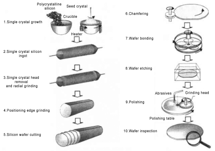
(2) Silicon wafer manufacturing:
Also known as chip manufacturing, the bare silicon wafer arrives at the silicon wafer manufacturing plant and then goes through various cleaning, film formation, photolithography, etching and doping steps. The processed silicon wafer has a complete set of integrated circuits permanently etched on the silicon wafer.
(3) Testing and selection of silicon wafers:
After silicon wafer manufacturing is completed, the silicon wafers are sent to the test/sort area, where individual chips are probed and electrically tested. Acceptable and unacceptable chips are then sorted out, and defective chips are marked.
(4) Assembly and packaging:
After wafer testing/sorting, the wafers enter the assembly and packaging step to package the individual chips in a protective tube package. The back side of the wafer is ground to reduce the thickness of the substrate.
A thick plastic film is attached to the back of each wafer, and then a diamond-tipped saw blade is used to separate the chips on each wafer along the scribe lines on the front side.
The plastic film on the back of the silicon wafer keeps the silicon chip from falling off. In the assembly plant, the good chips are pressed or evacuated to form an assembly package. Later, the chip is sealed in a plastic or ceramic shell.
(5) Final test:
To ensure the functionality of the chip, each packaged integrated circuit is tested to meet the manufacturer’s electrical and environmental characteristic parameter requirements. After final testing, the chip is sent to the customer for assembly in a dedicated location.
2.2 Process Division
Integrated circuit manufacturing processes are generally divided into:
Front-end: The front-end process generally refers to the manufacturing process of devices such as transistors, mainly including the formation processes of isolation, gate structure, source and drain, contact holes, etc.
Back-end: The back-end process mainly refers to the formation of interconnection lines that can transmit electrical signals to various devices on the chip, mainly including processes such as dielectric deposition between interconnection lines, metal line formation, and lead pad formation.
Mid-stage: In order to improve the performance of transistors, advanced technology nodes after 45nm/28nm use high-k gate dielectrics and metal gate processes, and add replacement gate processes and local interconnect processes after the transistor source and drain structure is prepared. These processes are between the front-end process and the back-end process, and are not used in traditional processes, so they are called mid-stage processes.
Usually, the contact hole preparation process is the dividing line between the front-end process and the back-end process.
Contact hole: a hole etched vertically in the silicon wafer to connect the first-layer metal interconnection line and the substrate device. It is filled with metal such as tungsten and is used to lead the device electrode to the metal interconnection layer.
Through Hole: It is the connection path between two adjacent layers of metal interconnect lines, located in the dielectric layer between the two metal layers, and is generally filled with metals such as copper.
In a broad sense:
Front-end process: In a broad sense, integrated circuit manufacturing should also include testing, packaging and other steps. Compared with testing and packaging, component and interconnect manufacturing are the first part of integrated circuit manufacturing, collectively referred to as front-end processes;
Back-end process: Testing and packaging are called back-end processes.
3. Appendix
SMIF:Standard Mechanical Interface
AMHS:Automated Material Handing System
OHT:Overhead Hoist Transfer
FOUP:Front Opening Unified Pod,Exclusive to 12 inch(300mm) wafers
More importantly, Semicera can provide graphite parts, soft/rigid felt, silicon carbide parts, CVD silicon carbide parts, and SiC/TaC coated parts with full semiconductor process in 30 days.We sincerely look forward to becoming your long-term partner in China.
Post time: Aug-15-2024