Hundreds of processes are required to turn a wafer into a semiconductor. One of the most important processes is etching - that is, carving fine circuit patterns on the wafer. The success of the etching process depends on managing various variables within a set distribution range, and each etching equipment must be prepared to operate under optimal conditions. Our etching process engineers use superb manufacturing technology to complete this detailed process.
SK Hynix News Center interviewed members of the Icheon DRAM Front Etch, Middle Etch, and End Etch technical teams to learn more about their work.
Etch: A Journey to Productivity Improvement
In semiconductor manufacturing, etching refers to carving patterns on thin films. The patterns are sprayed using plasma to form the final outline of each process step. Its main purpose is to perfectly present precise patterns according to the layout and maintain uniform results under all conditions.
If problems occur in the deposition or photolithography process, they can be solved by selective etching (Etch) technology. However, if something goes wrong during the etching process, the situation cannot be reversed. This is because the same material cannot be filled in the engraved area. Therefore, in the semiconductor manufacturing process, etching is crucial to determine the overall yield and product quality.
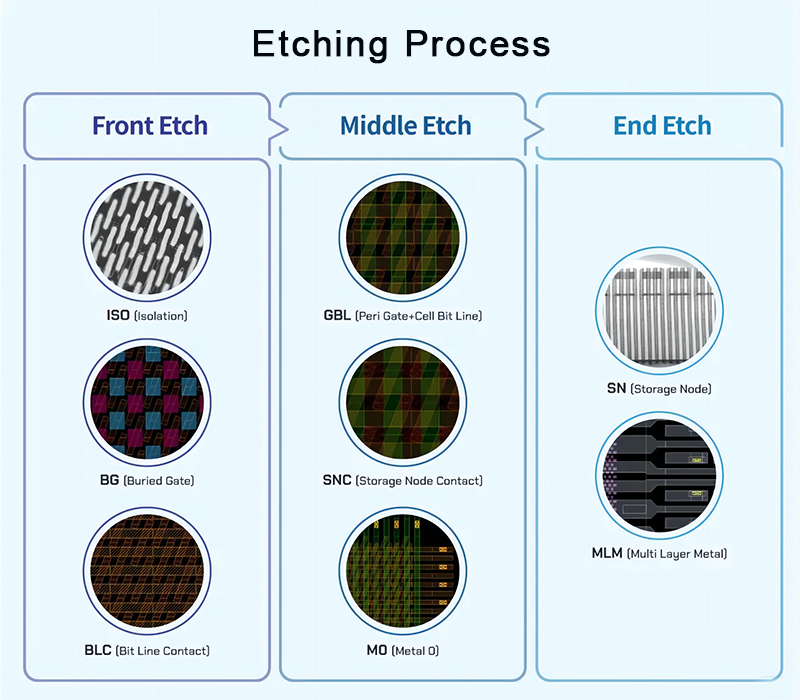
The etching process includes eight steps: ISO, BG, BLC, GBL, SNC, M0, SN and MLM.
First, the ISO (Isolation) stage etches (Etch) silicon (Si) on the wafer to create the active cell area. The BG (Buried Gate) stage forms the row address line (Word Line) 1 and the gate to create an electronic channel. Next, the BLC (Bit Line Contact) stage creates the connection between the ISO and the column address line (Bit Line) 2 in the cell area. The GBL (Peri Gate+Cell Bit Line) stage will simultaneously create the cell column address line and the gate in the periphery 3.
The SNC (Storage Node Contract) stage continues to create the connection between the active area and the storage node 4. Subsequently, the M0 (Metal0) stage forms the connection points of the peripheral S/D (Storage Node) 5 and the connection points between the column address line and the storage node. The SN (Storage Node) stage confirms the unit capacity, and the subsequent MLM (Multi Layer Metal) stage creates the external power supply and internal wiring, and the entire etching (Etch) engineering process is completed.
Given that etching (Etch) technicians are mainly responsible for the patterning of semiconductors, the DRAM department is divided into three teams: Front Etch (ISO, BG, BLC); Middle Etch (GBL, SNC, M0); End Etch (SN, MLM). These teams are also divided according to manufacturing positions and equipment positions.
Manufacturing positions are responsible for managing and improving unit production processes. Manufacturing positions play a very important role in improving yield and product quality through variable control and other production optimization measures.
Equipment positions are responsible for managing and strengthening production equipment to avoid problems that may occur during the etching process. The core responsibility of equipment positions is to ensure the optimal performance of equipment.
Although the responsibilities are clear, all teams work towards a common goal – that is, to manage and improve production processes and related equipment to improve productivity. To this end, each team actively shares their own achievements and areas for improvement, and cooperates to improve business performance.
How to cope with the challenges of miniaturization technology
SK Hynix began mass production of 8Gb LPDDR4 DRAM products for 10nm (1a) class process in July 2021.
Semiconductor memory circuit patterns have entered the 10nm era, and after improvements, a single DRAM can accommodate about 10,000 cells. Therefore, even in the etching process, the process margin is insufficient.
If the formed hole (Hole) 6 is too small, it may appear “unopened” and block the lower part of the chip. In addition, if the formed hole is too large, “bridging” may occur. When the gap between two holes is insufficient, “bridging” occurs, resulting in mutual adhesion problems in subsequent steps. As semiconductors become increasingly refined, the range of hole size values is gradually shrinking, and these risks will gradually be eliminated.
To solve the above problems, etching technology experts continue to improve the process, including modifying the process recipe and APC7 algorithm, and introducing new etching technologies such as ADCC8 and LSR9.
As customer needs become more diverse, another challenge has emerged – the trend of multi-product production. To meet such customer needs, the optimized process conditions for each product need to be set separately. This is a very special challenge for engineers because they need to make mass production technology meet the needs of both established conditions and diversified conditions.
To this end, Etch engineers introduced the “APC offset”10 technology to manage various derivatives based on core products (Core Products), and established and used the “T-index system” to comprehensively manage various products. Through these efforts, the system has been continuously improved to meet the needs of multi-product production.
Post time: Jul-16-2024