Overview of Semiconductor Process
The semiconductor process primarily involves applying microfabrication and film technologies to fully connect chips and other elements within various regions, such as substrates and frames. This facilitates the extraction of lead terminals and encapsulation with a plastic insulating medium to form an integrated whole, presented as a three-dimensional structure, ultimately completing the semiconductor packaging process. The concept of the semiconductor process also pertains to the narrow definition of semiconductor chip packaging. From a broader perspective, it refers to packaging engineering, which involves connecting and fixing to the substrate, configuring the corresponding electronic equipment, and constructing a complete system with strong comprehensive performance.
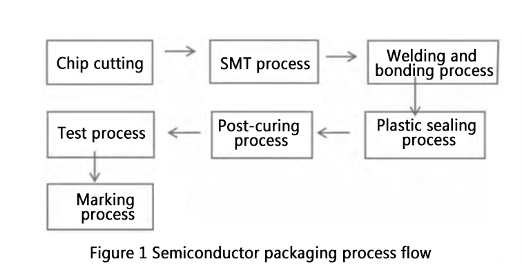
Semiconductor Packaging Process Flow
The semiconductor packaging process includes multiple tasks, as illustrated in Figure 1. Each process has specific requirements and closely related workflows, necessitating detailed analysis during the practical stage. The specific content is as follows:
1. Chip Cutting
In the semiconductor packaging process, chip cutting involves slicing silicon wafers into individual chips and promptly removing silicon debris to prevent hindrances to subsequent work and quality control.
2. Chip Mounting
The chip mounting process focuses on avoiding circuit damage during wafer grinding by applying a protective film layer, consistently emphasizing circuit integrity.
3. Wire Bonding Process
Controlling the quality of the wire bonding process involves using different types of gold wires to connect the chip’s bonding pads with the frame pads, ensuring the chip can connect to external circuits and maintaining overall process integrity. Typically, doped gold wires and alloyed gold wires are used.
Doped Gold Wires: Types include GS, GW, and TS, suitable for high-arc (GS: >250 μm), medium-high arc (GW: 200-300 μm), and medium-low arc (TS: 100-200 μm) bonding respectively.
Alloyed Gold Wires: Types include AG2 and AG3, suitable for low-arc bonding (70-100 μm).
The diameter options for these wires range from 0.013 mm to 0.070 mm. Selecting the appropriate type and diameter based on operational requirements and standards is crucial for quality control.
4. Molding Process
The main circuitry in molding elements involves encapsulation. Controlling the quality of the molding process protects the components, especially from external forces causing varying degrees of damage. This involves thorough analysis of the components’ physical properties.
Three main methods are currently used: ceramic packaging, plastic packaging, and traditional packaging. Managing the proportion of each packaging type is crucial to meet global chip production demands. During the process, comprehensive abilities are required, such as preheating the chip and lead frame before encapsulation with epoxy resin, molding, and post-mold curing.
5. Post-Curing Process
After the molding process, post-curing treatment is required, focusing on removing any excess materials around the process or package. Quality control is essential to avoid affecting overall process quality and appearance.
6.Testing Process
Once the previous processes are completed, the overall quality of the process must be tested using advanced testing technologies and facilities. This step involves detailed recording of data, focusing on whether the chip operates normally based on its performance level. Given the high cost of testing equipment, it’s crucial to maintain quality control throughout the production stages, including visual inspection and electrical performance testing.
Electrical Performance Testing: This involves testing integrated circuits using automatic test equipment and ensuring each circuit is properly connected for electrical testing.
Visual Inspection: Technicians use microscopes to thoroughly inspect the finished packaged chips to ensure they are free from defects and meet semiconductor packaging quality standards.
7. Marking Process
The marking process involves transferring the tested chips to a semi-finished warehouse for final processing, quality inspection, packaging, and shipping. This process includes three main steps:
1)Electroplating: After forming the leads, an anti-corrosion material is applied to prevent oxidation and corrosion. Electroplating deposition technology is typically used since most leads are made of tin.
2)Bending: The processed leads are then shaped, with the integrated circuit strip placed in a lead forming tool, controlling the lead shape (J or L type) and surface-mounted packaging.
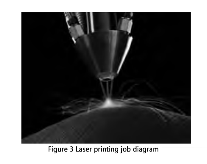
3)Laser Printing: Finally, the formed products are printed with a design, which serves as a special mark for the semiconductor packaging process, as illustrated in Figure 3.
Challenges and Recommendations
The study of semiconductor packaging processes begins with an overview of semiconductor technology to understand its principles. Next, examining the packaging process flow aims to ensure meticulous control during operations, using refined management to avoid routine issues. In the context of modern development, identifying challenges in semiconductor packaging processes is essential. It is recommended to focus on quality control aspects, thoroughly mastering key points to effectively enhance the process quality.
Analyzing from a quality control perspective, there are significant challenges during implementation due to numerous processes with specific content and requirements, each influencing the other. Rigorous control is needed during practical operations. By adopting a meticulous work attitude and applying advanced technologies, semiconductor packaging process quality and technical levels can be improved, ensuring comprehensive application effectiveness and achieving excellent overall benefits.(as shown in Figure 3).
Post time: May-22-2024