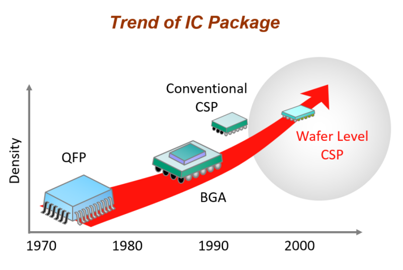
Packaging technology is one of the most important processes in the semiconductor industry. According to the shape of the package, it can be divided into socket package, surface mount package, BGA package, chip size package (CSP), single chip module package (SCM, the gap between the wiring on the printed circuit board (PCB) and the integrated circuit (IC) board pad matches), multi-chip module package (MCM, which can integrate heterogeneous chips), wafer level package (WLP, including fan-out wafer level package (FOWLP), micro surface mount components (microSMD), etc.), three-dimensional package (micro bump interconnect package, TSV interconnect package, etc.), system package (SIP), chip system (SOC).
The forms of 3D packaging are mainly divided into three categories: buried type (burying the device in multi-layer wiring or buried in the substrate), active substrate type (silicon wafer integration: first integrate the components and wafer substrate to form an active substrate; then arrange multi-layer interconnection lines, and assemble other chips or components on the top layer) and stacked type (silicon wafers stacked with silicon wafers, chips stacked with silicon wafers, and chips stacked with chips).
3D interconnection methods include wire bonding (WB), flip chip (FC), through silicon via (TSV), film conductor, etc.
TSV realizes vertical interconnection between chips. Since the vertical interconnection line has the shortest distance and higher strength, it is easier to realize miniaturization, high density, high performance, and multifunctional heterogeneous structure packaging. At the same time, it can also interconnect chips of different materials;
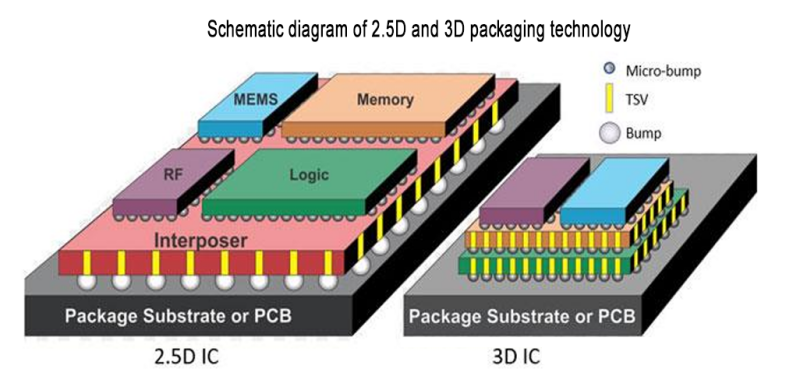
currently, there are two types of microelectronics manufacturing technologies using TSV process: three-dimensional circuit packaging (3D IC integration) and three-dimensional silicon packaging (3D Si integration).
The difference between the two forms is that:
(1) 3D circuit packaging requires the chip electrodes to be prepared into bumps, and the bumps are interconnected (bonded by bonding, fusion, welding, etc.), while 3D silicon packaging is a direct interconnection between chips (bonding between oxides and Cu-Cu bonding).
(2) 3D circuit integration technology can be achieved by bonding between wafers (3D circuit packaging, 3D silicon packaging), while chip-to-chip bonding and chip-to-wafer bonding can only be achieved by 3D circuit packaging.
(3) There are gaps between the chips integrated by the 3D circuit packaging process, and dielectric materials need to be filled to adjust the thermal conductivity and thermal expansion coefficient of the system to ensure the stability of the mechanical and electrical properties of the system; there are no gaps between the chips integrated by the 3D silicon packaging process, and the power consumption, volume, and weight of the chip are small, and the electrical performance is excellent.
The TSV process can construct a vertical signal path through the substrate and connect the RDL on the top and bottom of the substrate to form a three-dimensional conductor path. Therefore, the TSV process is one of the important cornerstones for constructing a three-dimensional passive device structure.
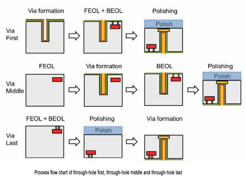
According to the order between the front end of line (FEOL) and the back end of line (BEOL), the TSV process can be divided into three mainstream manufacturing processes, namely, via first (ViaFirst), via middle (Via Middle) and via last (Via Last) process, as shown in the figure.
1. Via etching process
The via etching process is the key to manufacturing TSV structure. Choosing a suitable etching process can effectively improve the mechanical strength and electrical properties of TSV, and further related to the overall reliability of TSV three-dimensional devices.
At present, there are four main mainstream TSV via etching processes: Deep Reactive Ion Etching (DRIE), wet etching, photo-assisted electrochemical etching (PAECE) and laser drilling.
(1) Deep Reactive Ion Etching (DRIE)
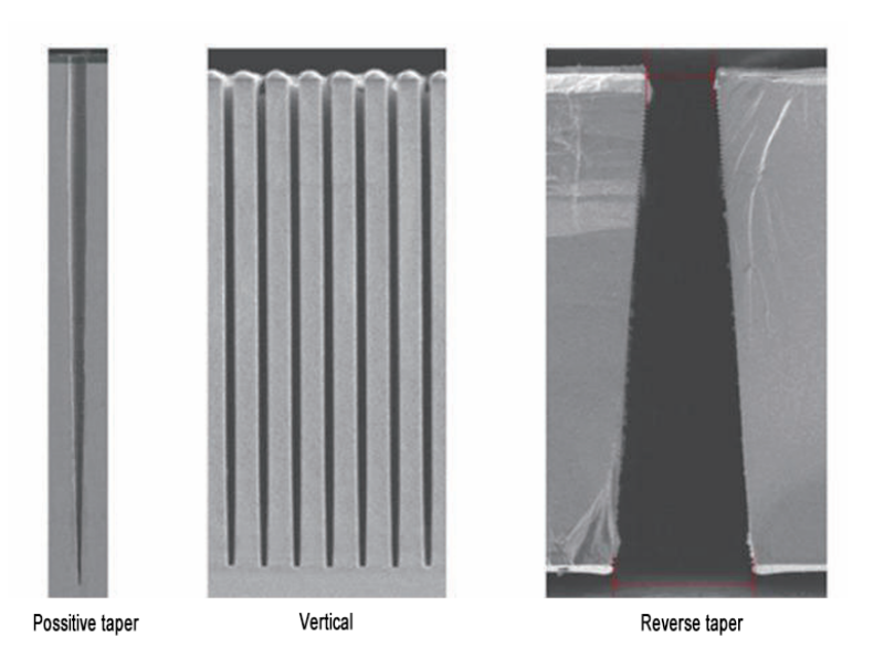
Deep reactive ion etching, also known as DRIE process, is the most commonly used TSV etching process, which is mainly used to realize TSV via structures with high aspect ratio. Traditional plasma etching processes can generally only achieve an etching depth of several microns, with a low etching rate and lack of etching mask selectivity. Bosch has made corresponding process improvements on this basis. By using SF6 as a reactive gas and releasing C4F8 gas during the etching process as a passivation protection for the sidewalls, the improved DRIE process is suitable for etching high aspect ratio vias. Therefore, it is also called the Bosch process after its inventor.
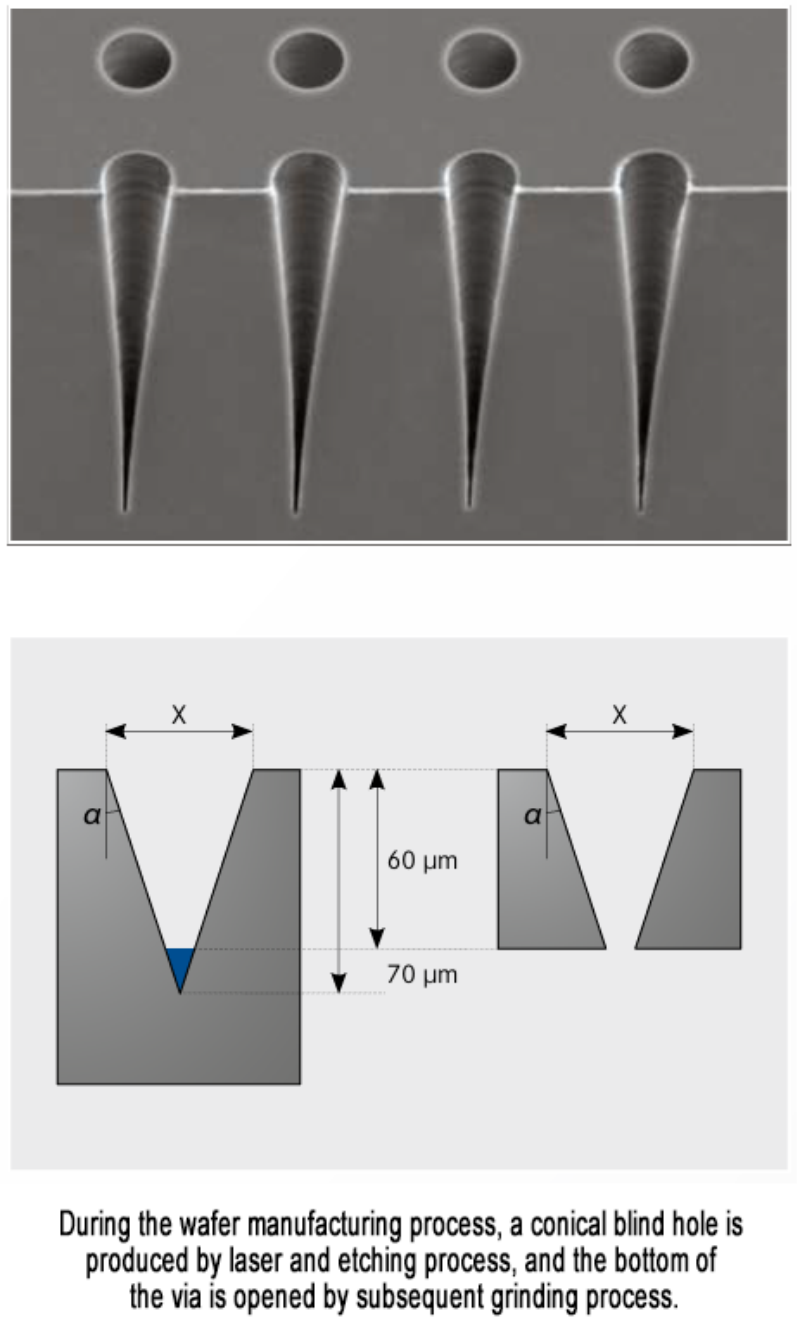
The figure below is a photo of a high aspect ratio via formed by etching the DRIE process.
Although the DRIE process is widely used in the TSV process due to its good controllability, its disadvantage is that the sidewall flatness is poor and scallop-shaped wrinkle defects will be formed. This defect is more significant when etching high aspect ratio vias.
(2) Wet etching
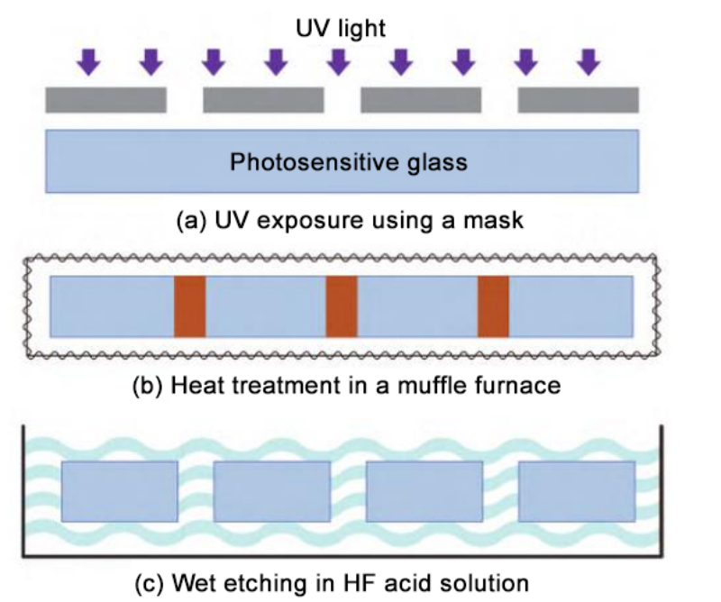
Wet etching uses a combination of mask and chemical etching to etch through holes. The most commonly used etching solution is KOH, which can etch the positions on the silicon substrate that are not protected by the mask, thereby forming the desired through-hole structure. Wet etching is the earliest through-hole etching process developed. Since its process steps and required equipment are relatively simple, it is suitable for mass production of TSV at low cost. However, its chemical etching mechanism determines that the through-hole formed by this method will be affected by the crystal orientation of the silicon wafer, making the etched through-hole non-vertical but showing a clear phenomenon of wide top and narrow bottom. This defect limits the application of wet etching in TSV manufacturing.
(3) Photo-assisted electrochemical etching (PAECE)
The basic principle of photo-assisted electrochemical etching (PAECE) is to use ultraviolet light to accelerate the generation of electron-hole pairs, thereby accelerating the electrochemical etching process. Compared with the widely used DRIE process, the PAECE process is more suitable for etching ultra-large aspect ratio through-hole structures greater than 100:1, but its disadvantage is that the controllability of etching depth is weaker than DRIE, and its technology may require further research and process improvement.
(4) Laser drilling
Is different from the above three methods. The laser drilling method is a purely physical method. It mainly uses high-energy laser irradiation to melt and evaporate the substrate material in the specified area to physically realize the through-hole construction of TSV.
The through-hole formed by laser drilling has a high aspect ratio and the sidewall is basically vertical. However, since laser drilling actually uses local heating to form the through-hole, the hole wall of TSV will be negatively affected by thermal damage and reduce reliability.
2. Liner layer deposition process
Another key technology for manufacturing TSV is the liner layer deposition process.
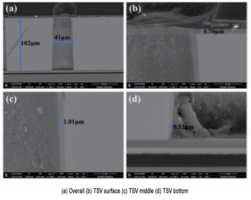
The liner layer deposition process is performed after the through-hole is etched. The deposited liner layer is generally an oxide such as SiO2. The liner layer is located between the internal conductor of the TSV and the substrate, and mainly plays the role of isolating DC current leakage. In addition to depositing oxide, barrier and seed layers are also required for conductor filling in the next process.
The manufactured liner layer must meet the following two basic requirements:
(1) the breakdown voltage of the insulating layer should meet the actual working requirements of TSV;
(2) the deposited layers are highly consistent and have good adhesion to each other.
The following figure shows a photo of the liner layer deposited by plasma enhanced chemical vapor deposition (PECVD).
The deposition process needs to be adjusted accordingly for different TSV manufacturing processes. For the front through-hole process, a high-temperature deposition process can be used to improve the quality of the oxide layer.
Typical high-temperature deposition can be based on tetraethyl orthosilicate (TEOS) combined with thermal oxidation process to form a highly consistent high-quality SiO2 insulating layer. For the middle through-hole and back through-hole process, since the BEOL process has been completed during deposition, a low-temperature method is required to ensure compatibility with BEOL materials.
Under this condition, the deposition temperature should be limited to 450°, including the use of PECVD to deposit SiO2 or SiNx as an insulating layer.
Another common method is to use atomic layer deposition (ALD) to deposit Al2O3 to obtain a denser insulating layer.
3. Metal filling process
The TSV filling process is carried out immediately after the liner deposition process, which is another key technology that determines the quality of TSV.
The materials that can be filled include doped polysilicon, tungsten, carbon nanotubes, etc. depending on the process used, but the most mainstream is still electroplated copper, because its process is mature and its electrical and thermal conductivity are relatively high.
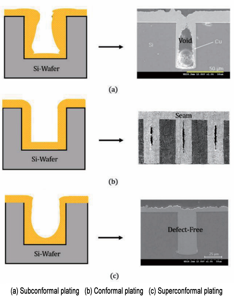
According to the distribution difference of its electroplating rate in the through hole, it can be mainly divided into subconformal, conformal, superconformal and bottom-up electroplating methods, as shown in the figure.
Subconformal electroplating was mainly used in the early stage of TSV research. As shown in Figure (a), the Cu ions provided by electrolysis are concentrated at the top, while the bottom is insufficiently supplemented, which causes the electroplating rate at the top of the through-hole to be higher than that below the top. Therefore, the top of the through-hole will be closed in advance before it is completely filled, and a large void will be formed inside.
The schematic diagram and photo of the conformal electroplating method are shown in Figure (b). By ensuring the uniform supplementation of Cu ions, the electroplating rate at each position in the through-hole is basically the same, so only a seam will be left inside, and the void volume is much smaller than that of the subconformal electroplating method, so it is widely used.
In order to further achieve a void-free filling effect, the superconformal electroplating method was proposed to optimize the conformal electroplating method. As shown in Figure (c), by controlling the supply of Cu ions, the filling rate at the bottom is slightly higher than that at other positions, thereby optimizing the step gradient of the filling rate from bottom to top to completely eliminate the seam left by the conformal electroplating method, so as to achieve completely void-free metal copper filling.
The bottom-up electroplating method can be considered as a special case of the super-conformal method. In this case, the electroplating rate except the bottom is suppressed to zero, and only the electroplating is gradually carried out from the bottom to the top. In addition to the void-free advantage of the conformal electroplating method, this method can also effectively reduce the overall electroplating time, so it has been widely studied in recent years.
4. RDL process technology
The RDL process is an indispensable basic technology in the three-dimensional packaging process. Through this process, metal interconnections can be manufactured on both sides of the substrate to achieve the purpose of port redistribution or interconnection between packages. Therefore, the RDL process is widely used in fan-in-fan-out or 2.5D/3D packaging systems.
In the process of building three-dimensional devices, the RDL process is usually used to interconnect TSV to realize a variety of three-dimensional device structures.
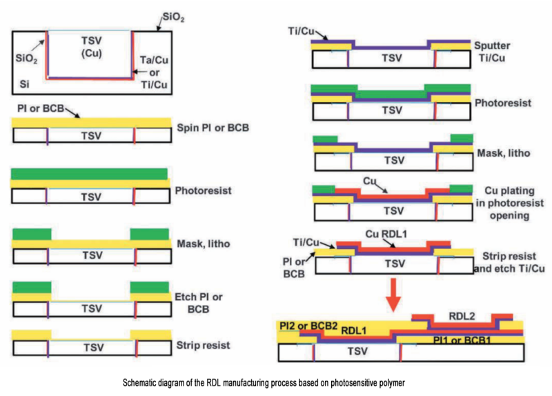
There are currently two main mainstream RDL processes. The first is based on photosensitive polymers and combined with copper electroplating and etching processes; the other is implemented by using Cu Damascus process combined with PECVD and chemical mechanical polishing (CMP) process.
The following will introduce the mainstream process paths of these two RDLs respectively.
The RDL process based on photosensitive polymer is shown in the figure above.
First, a layer of PI or BCB glue is coated on the surface of the wafer by rotation, and after heating and curing, a photolithography process is used to open holes at the desired position, and then etching is performed. Next, after removing the photoresist, Ti and Cu are sputtered on the wafer through a physical vapor deposition process (PVD) as a barrier layer and a seed layer, respectively. Next, the first layer of RDL is manufactured on the exposed Ti/Cu layer by combining photolithography and electroplating Cu processes, and then the photoresist is removed and the excess Ti and Cu are etched away. Repeat the above steps to form a multi-layer RDL structure. This method is currently more widely used in the industry.
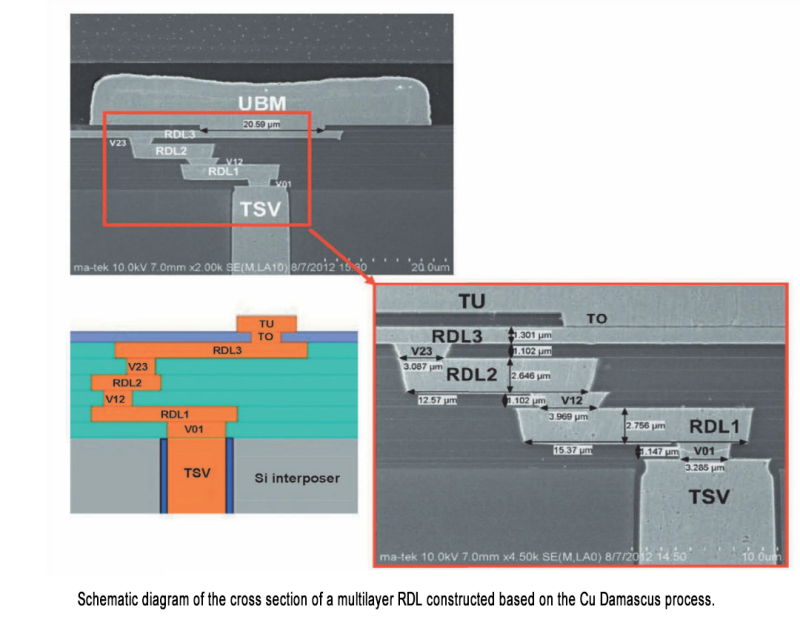
Another method for manufacturing RDL is mainly based on the Cu Damascus process, which combines PECVD and CMP processes.
The difference between this method and the RDL process based on photosensitive polymer is that in the first step of manufacturing each layer, PECVD is used to deposit SiO2 or Si3N4 as an insulating layer, and then a window is formed on the insulating layer by photolithography and reactive ion etching, and Ti/Cu barrier/seed layer and conductor copper are sputtered respectively, and then the conductor layer is thinned to the required thickness by CMP process, that is, a layer of RDL or through-hole layer is formed.
The following figure is a schematic diagram and photo of the cross-section of a multi-layer RDL constructed based on the Cu Damascus process. It can be observed that TSV is first connected to the through-hole layer V01, and then stacked from bottom to top in the order of RDL1, through-hole layer V12, and RDL2.
Each layer of RDL or through-hole layer is manufactured in sequence according to the above method.Since the RDL process requires the use of CMP process, its manufacturing cost is higher than that of the RDL process based on photosensitive polymer, so its application is relatively low.
5. IPD process technology
For the manufacture of three-dimensional devices, in addition to direct on-chip integration on MMIC, the IPD process provides another more flexible technical path.
Integrated passive devices, also known as IPD process, integrate any combination of passive devices including on-chip inductors, capacitors, resistors, balun converters, etc. on a separate substrate to form a passive device library in the form of a transfer board that can be flexibly called according to design requirements.
Since in the IPD process, passive devices are manufactured and directly integrated on the transfer board, its process flow is simpler and less expensive than on-chip integration of ICs, and can be mass-produced in advance as a passive device library.
For TSV three-dimensional passive device manufacturing, IPD can effectively offset the cost burden of three-dimensional packaging processes including TSV and RDL.
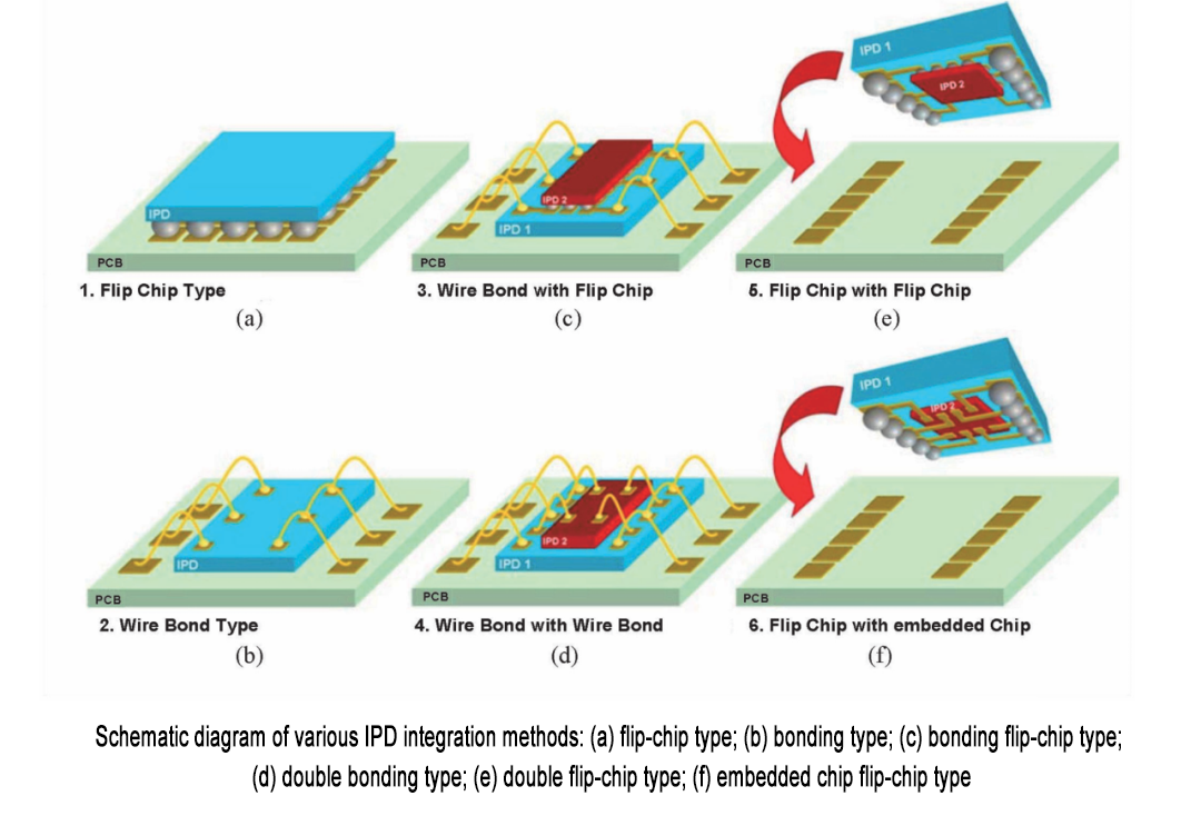
In addition to cost advantages, another advantage of IPD is its high flexibility. One of the flexibility of IPD is reflected in the diverse integration methods, as shown in the figure below. In addition to the two basic methods of directly integrating IPD into the package substrate through the flip-chip process as shown in Figure (a) or the bonding process as shown in Figure (b), another layer of IPD can be integrated on one layer of IPD as shown in Figures (c)-(e) to achieve a wider range of passive device combinations.
At the same time, as shown in Figure (f), the IPD can be further used as an adapter board to directly bury the integrated chip on it to directly build a high-density packaging system.
When using IPD to build three-dimensional passive devices, TSV process and RDL process can also be used. The process flow is basically the same as the above-mentioned on-chip integration processing method, and will not be repeated; the difference is that since the object of integration is changed from chip to adapter board, there is no need to consider the impact of the three-dimensional packaging process on the active area and interconnection layer. This further leads to another key flexibility of IPD: a variety of substrate materials can be flexibly selected according to the design requirements of passive devices.
The substrate materials available for IPD are not only common semiconductor substrate materials such as Si and GaN, but also Al2O3 ceramics, low-temperature/high-temperature co-fired ceramics, glass substrates, etc. This feature effectively expands the design flexibility of passive devices integrated by IPD.
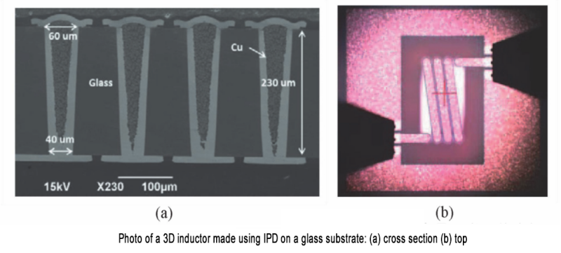
For example, the three-dimensional passive inductor structure integrated by IPD can use a glass substrate to effectively improve the performance of the inductor. In contrast to the concept of TSV, the through-holes made on the glass substrate are also called through-glass vias (TGV). The photo of the three-dimensional inductor manufactured based on IPD and TGV processes is shown in the figure below. Since the resistivity of the glass substrate is much higher than that of conventional semiconductor materials such as Si, the TGV three-dimensional inductor has better insulation properties, and the insertion loss caused by the substrate parasitic effect at high frequencies is much smaller than that of the conventional TSV three-dimensional inductor.
On the other hand, metal-insulator-metal (MIM) capacitors can also be manufactured on the glass substrate IPD through a thin film deposition process, and interconnected with the TGV three-dimensional inductor to form a three-dimensional passive filter structure. Therefore, the IPD process has broad application potential for the development of new three-dimensional passive devices.
Post time: Nov-12-2024

