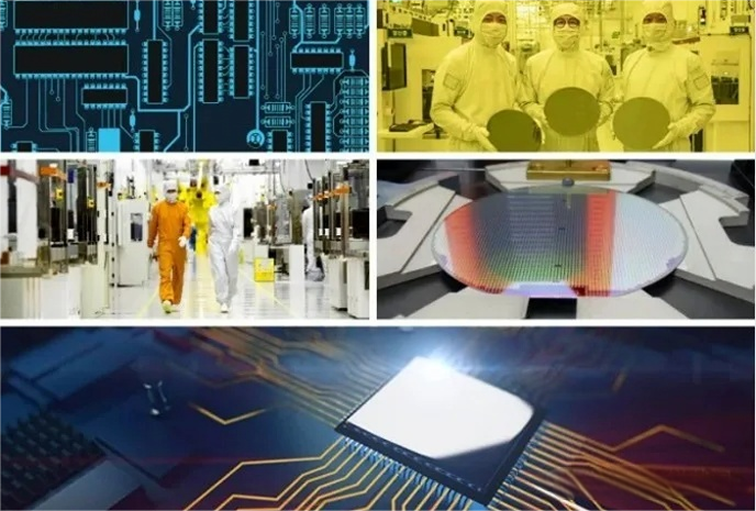
The front, middle and back ends of semiconductor manufacturing production lines
The semiconductor manufacturing process can be roughly divided into three stages:
1) Front end of line
2) Mid end of line
3) Back end of line
We can use a simple analogy like building a house to explore the complex process of chip manufacturing:
The front end of the production line is like laying the foundation and building the walls of a house. In semiconductor manufacturing, this stage involves creating the basic structures and transistors on a silicon wafer.
Key Steps of FEOL:
1.Cleaning: Start with a thin silicon wafer and clean it to remove any impurities.
2.Oxidation: Grow a layer of silicon dioxide on the wafer to isolate different parts of the chip.
3.Photolithography: Use photolithography to etch patterns onto the wafer, akin to drawing blueprints with light.
4.Etching: Etch away unwanted silicon dioxide to reveal the desired patterns.
5.Doping: Introduce impurities into the silicon to alter its electrical properties, creating transistors, the fundamental building blocks of any chip.
Mid End of Line (MEOL): Connecting the Dots
The mid end of the production line is like installing wiring and plumbing in a house. This stage focuses on establishing connections between the transistors created in the FEOL stage.
Key Steps of MEOL:
1.Dielectric Deposition: Deposit insulating layers (called dielectrics) to protect the transistors.
2.Contact Formation: Form contacts to connect the transistors to each other and the outside world.
3.Interconnect: Add metal layers to create pathways for electrical signals, similar to wiring a house to ensure seamless power and data flow.
Back End of Line (BEOL): Finishing Touches
The back end of the production line is like adding the final touches to a house—installing fixtures, painting, and ensuring everything works. In semiconductor manufacturing, this stage involves adding the final layers and preparing the chip for packaging.
Key Steps of BEOL:
1.Additional Metal Layers: Add multiple metal layers to enhance interconnectivity, ensuring the chip can handle complex tasks and high speeds.
2.Passivation: Apply protective layers to shield the chip from environmental damage.
3.Testing: Subject the chip to rigorous testing to ensure it meets all specifications.
4.Dicing: Cut the wafer into individual chips, each ready for packaging and use in electronic devices.
Semicera is a leading OEM manufacturer in China, dedicated to providing exceptional value to our customers. We offer a comprehensive range of high-quality products and services, including:
1.CVD SiC Coating (Epitaxy, custom CVD-coated parts, high-performance coatings for semiconductor applications, and more)
2.CVD SiC Bulk Parts (Etch rings, focus rings, custom SiC components for semiconductor equipment, and more)
3.CVD TaC Coated Parts (Epitaxy, SiC wafer growth, high-temperature applications, and more)
4.Graphite Parts (Graphite boats, custom graphite components for high-temperature processing, and more)
5.SiC Parts (SiC boats, SiC furnace tubes, custom SiC components for advanced material processing, and more)
6.Quartz Parts (Quartz boats, custom quartz parts for semiconductor and solar industries, and more)
Our commitment to excellence ensures we provide innovative and reliable solutions for various industries, including semiconductor manufacturing, advanced materials processing, and high-tech applications. With a focus on precision and quality, we are dedicated to meeting the unique needs of each customer.
Post time: Dec-09-2024