Semiconductor power devices occupy a core position in power electronic systems, especially in the context of the rapid development of technologies such as artificial intelligence, 5G communications and new energy vehicles, the performance requirements for them have been improved.
Silicon carbide (4H-SiC) has become an ideal material for manufacturing high-performance semiconductor power devices due to its advantages such as wide bandgap, high thermal conductivity, high breakdown field strength, high saturation drift rate, chemical stability and radiation resistance. However, 4H-SiC has high hardness, high brittleness, strong chemical inertness, and high processing difficulty. The surface quality of its substrate wafer is crucial for large-scale device applications.
Therefore, improving the surface quality of 4H-SiC substrate wafers, especially removing the damaged layer on the wafer processing surface, is the key to achieving efficient, low-loss and high-quality 4H-SiC substrate wafer processing.
Experiment
The experiment uses a 4-inch N-type 4H-SiC ingot grown by physical vapor transport method, which is processed through wire cutting, grinding, rough grinding, fine grinding and polishing, and records the removal thickness of the C surface and Si surface and the final wafer thickness in each process.
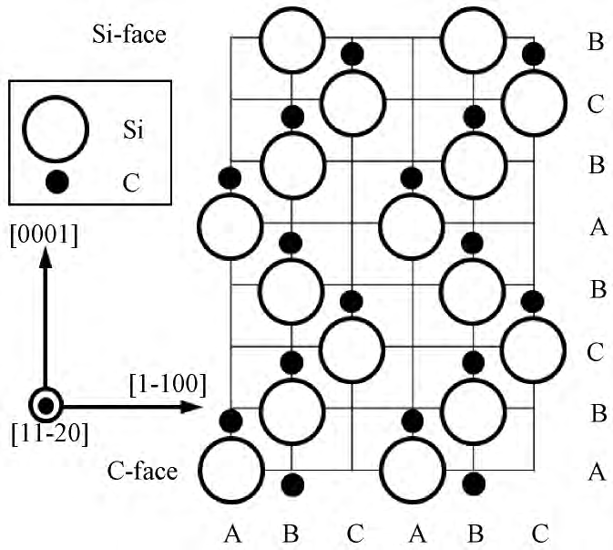
Figure 1 Schematic diagram of 4H-SiC crystal structure
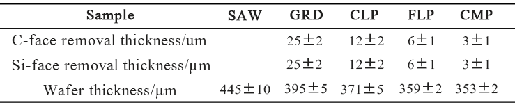
Figure 2 Thickness removed from C-side and Si-side of 4H-SiC wafer after different processing steps and thickness of wafer after processing
The thickness, surface morphology, roughness and mechanical properties of the wafer were fully characterized by wafer geometry parameter tester, differential interference microscope, atomic force microscope, surface roughness measuring instrument and nanoindenter. In addition, high-resolution X-ray diffractometer was used to evaluate the crystal quality of the wafer.
These experimental steps and test methods provide detailed technical support for studying the material removal rate and surface quality during the processing of 4H-SiC wafers.
Through experiments, the researchers analyzed the changes in material removal rate (MRR), surface morphology and roughness, as well as mechanical properties and crystal quality of 4H-SiC wafers in different processing steps (wire cutting, grinding, rough grinding, fine grinding, polishing).
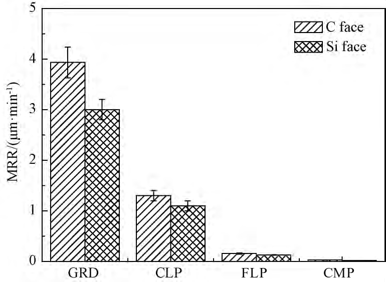
Figure 3 Material removal rate of C-face and Si-face of 4H-SiC wafer in different processing steps
The study found that due to the anisotropy of mechanical properties of different crystal faces of 4H-SiC, there is a difference in MRR between C-face and Si-face under the same process, and the MRR of C-face is significantly higher than that of Si-face. With the advancement of the processing steps, the surface morphology and roughness of 4H-SiC wafers are gradually optimized. After polishing, the Ra of C-face is 0.24nm, and the Ra of Si-face reaches 0.14nm, which can meet the needs of epitaxial growth.
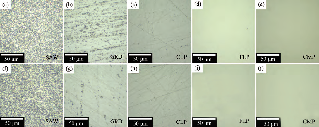
Figure 4 Optical microscope images of the C surface (a~e) and Si surface (f~j) of 4H-SiC wafer after different processing steps
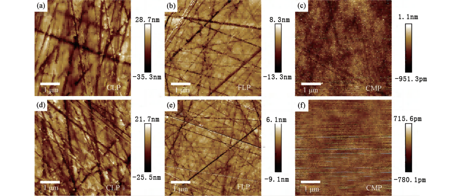
Figure 5 Atomic force microscope images of the C surface (a~c) and Si surface (d~f) of 4H-SiC wafer after CLP, FLP and CMP processing steps
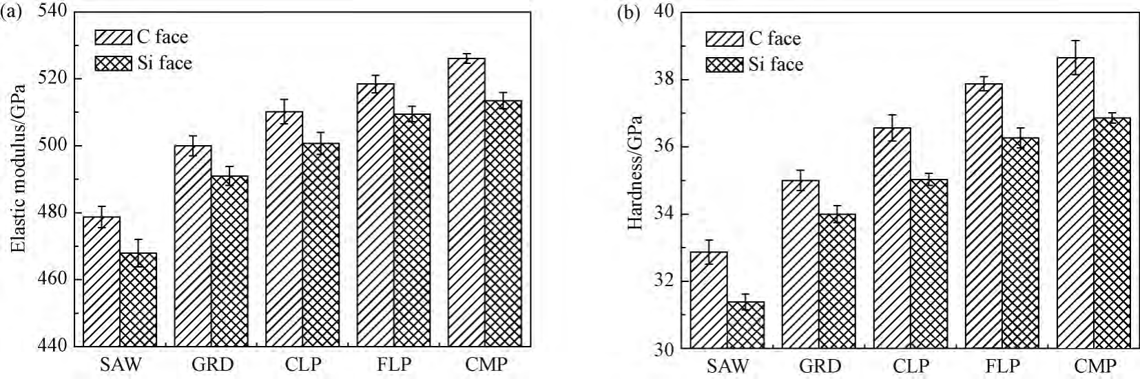
Figure 6 (a) elastic modulus and (b) hardness of the C surface and Si surface of 4H-SiC wafer after different processing steps
The mechanical property test shows that the C surface of the wafer has poorer toughness than the Si surface material, a greater degree of brittle fracture during processing, faster material removal, and relatively poor surface morphology and roughness. Removing the damaged layer on the processed surface is the key to improving the surface quality of the wafer. The half-height width of the 4H-SiC (0004) rocking curve can be used to intuitively and accurately characterize and analyze the surface damage layer of the wafer.
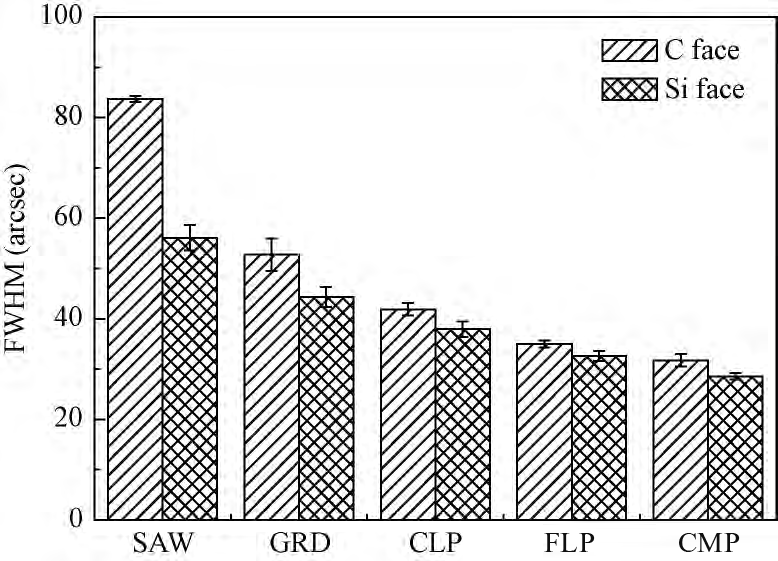
Figure 7 (0004) rocking curve half-width of the C-face and Si-face of 4H-SiC wafer after different processing steps
The research results show that the surface damage layer of the wafer can be gradually removed after 4H-SiC wafer processing, which effectively improves the surface quality of the wafer and provides a technical reference for high-efficiency, low-loss and high-quality processing of 4H-SiC substrate wafers.
The researchers processed 4H-SiC wafers through different processing steps such as wire cutting, grinding, rough grinding, fine grinding and polishing, and studied the effects of these processes on the surface quality of the wafer.
The results show that with the advancement of the processing steps, the surface morphology and roughness of the wafer are gradually optimized. After polishing, the roughness of the C-face and Si-face reaches 0.24nm and 0.14nm respectively, which meets the requirements of epitaxial growth. The C-face of the wafer has poorer toughness than the Si-face material, and is more prone to brittle fracture during processing, resulting in relatively poor surface morphology and roughness. Removing the surface damage layer of the processed surface is the key to improving the surface quality of the wafer. The half-width of the 4H-SiC (0004) rocking curve can intuitively and accurately characterize the surface damage layer of the wafer.
Research shows that the damaged layer on the surface of 4H-SiC wafers can be gradually removed through 4H-SiC wafer processing, effectively improving the surface quality of the wafer, providing a technical reference for high-efficiency, low-loss, and high-quality processing of 4H-SiC substrate wafers.
Post time: Jul-08-2024