Dry etching process usually consists of four basic states: before etching, partial etching, just etching, and over etching. The main characteristics are etching rate, selectivity, critical dimension, uniformity, and endpoint detection.
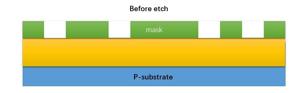
Figure 1 Before etching
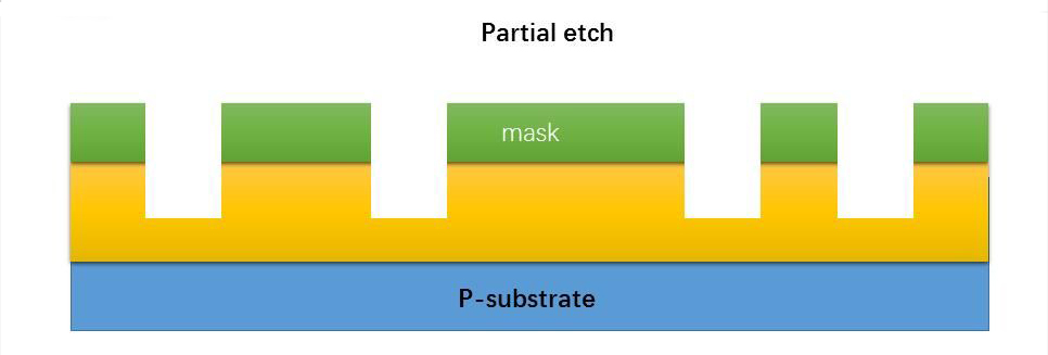
Figure 2 Partial etching
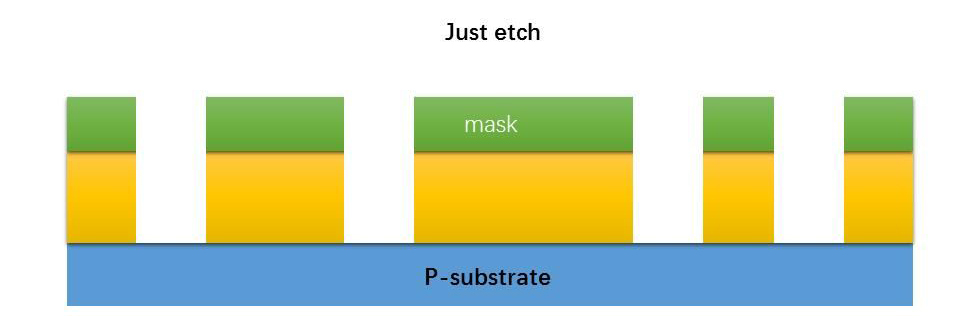
Figure 3 Just etching
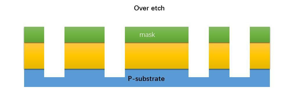
Figure 4 Over etching
(1) Etching rate: the depth or thickness of the etched material removed per unit time.
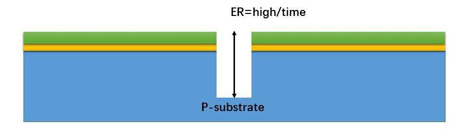
Figure 5 Etching rate diagram
(2) Selectivity: the ratio of etching rates of different etching materials.
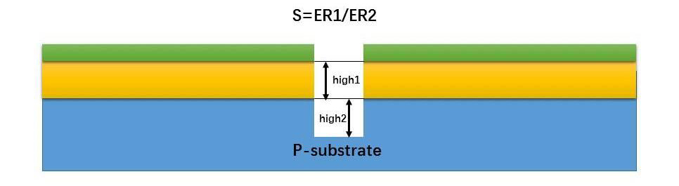
Figure 6 Selectivity diagram
(3) Critical dimension: the size of the pattern in a specific area after etching is completed.
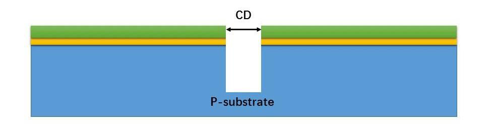
Figure 7 Critical dimension diagram
(4) Uniformity: to measure the uniformity of the critical etching dimension (CD), generally characterized by the full map of CD, the formula is: U=(Max-Min)/2*AVG.
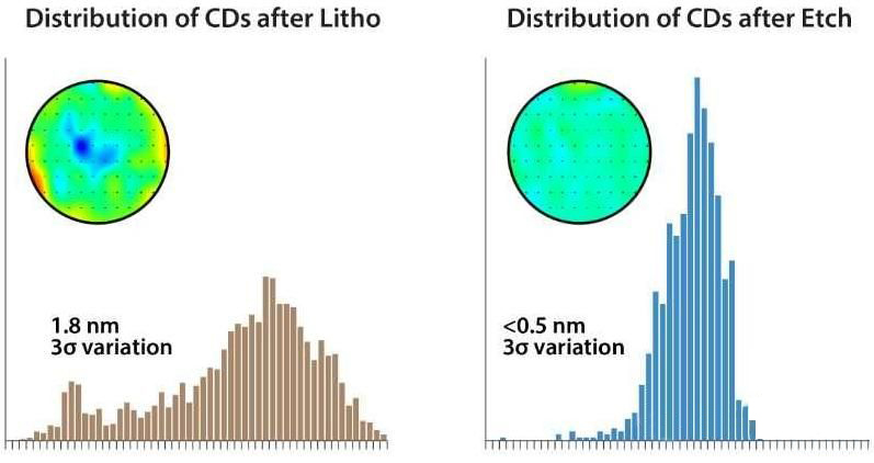
Figure 8 Uniformity Schematic Diagram
(5) End point detection: During the etching process, the change of light intensity is constantly detected. When a certain light intensity rises or falls significantly, the etching is terminated to mark the completion of a certain layer of film etching.
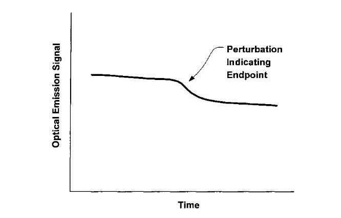
Figure 9 End point schematic diagram
In dry etching, the gas is excited by high frequency (mainly 13.56 MHz or 2.45 GHz). At a pressure of 1 to 100 Pa, its mean free path is several millimeters to several centimeters. There are three main types of dry etching:
• Physical dry etching: accelerated particles physically wear the wafer surface
• Chemical dry etching: gas reacts chemically with the wafer surface
• Chemical physical dry etching: physical etching process with chemical characteristics
1. Ion beam etching
Ion beam etching (Ion Beam Etching) is a physical dry processing process that uses a high-energy argon ion beam with an energy of about 1 to 3 keV to irradiate the material surface. The energy of the ion beam causes it to impact and remove the surface material. The etching process is anisotropic in the case of vertical or oblique incident ion beams. However, due to its lack of selectivity, there is no clear distinction between materials at different levels. The generated gases and the etched materials are exhausted by the vacuum pump, but since the reaction products are not gases, particles are deposited on the wafer or chamber walls.
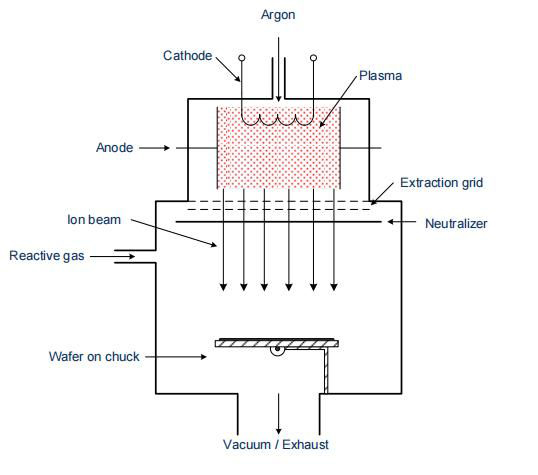
To prevent the formation of particles, a second gas can be introduced into the chamber. This gas will react with the argon ions and cause a physical and chemical etching process. Part of the gas will react with the surface material, but it will also react with the polished particles to form gaseous byproducts. Almost all kinds of materials can be etched by this method. Due to the vertical radiation, the wear on the vertical walls is very small (high anisotropy). However, due to its low selectivity and slow etching rate, this process is rarely used in current semiconductor manufacturing.
2. Plasma etching
Plasma etching is an absolute chemical etching process, also known as chemical dry etching. Its advantage is that it does not cause ion damage to the wafer surface. Since the active species in the etching gas are free to move and the etching process is isotropic, this method is suitable for removing the entire film layer (for example, cleaning the back side after thermal oxidation).
A downstream reactor is a type of reactor commonly used for plasma etching. In this reactor, the plasma is generated by impact ionization in a high-frequency electric field of 2.45GHz and separated from the wafer.
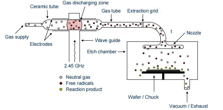
In the gas discharge area, various particles are generated due to impact and excitation, including free radicals. Free radicals are neutral atoms or molecules with unsaturated electrons, so they are highly reactive. In the plasma etching process, some neutral gases, such as tetrafluoromethane (CF4), are often used, which are introduced into the gas discharge area to generate active species by ionization or decomposition.
For example, in CF4 gas, it is introduced into the gas discharge area and decomposed into fluorine radicals (F) and carbon difluoride molecules (CF2). Similarly, fluorine (F) can be decomposed from CF4 by adding oxygen (O2).
2 CF4 + O2 —> 2 COF2 + 2 F2
The fluorine molecule can split into two independent fluorine atoms under the energy of the gas discharge region, each of which is a fluorine free radical. Since each fluorine atom has seven valence electrons and tends to achieve the electronic configuration of an inert gas, they are all very reactive. In addition to neutral fluorine free radicals, there will be charged particles such as CF+4, CF+3, CF+2, etc. in the gas discharge region. Subsequently, all these particles and free radicals are introduced into the etching chamber through the ceramic tube.
The charged particles can be blocked by extraction gratings or recombined in the process of forming neutral molecules to control their behavior in the etching chamber. Fluorine free radicals will also undergo partial recombination, but are still active enough to enter the etching chamber, react chemically on the wafer surface and cause material stripping. Other neutral particles do not participate in the etching process and are consumed along with the reaction products.
Examples of thin films that can be etched in plasma etching:
• Silicon: Si + 4F—> SiF4
• Silicon dioxide: SiO2 + 4F—> SiF4 + O2
• Silicon nitride: Si3N4 + 12F—> 3SiF4 + 2N2
3.Reactive ion etching (RIE)
Reactive ion etching is a chemical-physical etching process that can very accurately control selectivity, etching profile, etching rate, uniformity and repeatability. It can achieve isotropic and anisotropic etching profiles and is therefore one of the most important processes for building various thin films in semiconductor manufacturing.
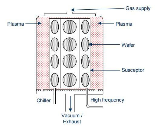
During RIE, the wafer is placed on a high-frequency electrode (HF electrode). Through impact ionization, a plasma is generated in which free electrons and positively charged ions exist. If a positive voltage is applied to the HF electrode, the free electrons accumulate on the electrode surface and cannot leave the electrode again due to their electron affinity. Therefore, the electrodes are charged to -1000V (bias voltage) so that the slow ions cannot follow the rapidly changing electric field to the negatively charged electrode.
During ion etching (RIE), if the mean free path of the ions is high, they hit the wafer surface in an almost perpendicular direction. In this way, the accelerated ions knock out the material and form a chemical reaction through physical etching. Since the lateral sidewalls are not affected, the etch profile remains anisotropic and the surface wear is small. However, the selectivity is not very high because the physical etching process also occurs. In addition, the acceleration of the ions causes damage to the wafer surface, which requires thermal annealing to repair.
The chemical part of the etching process is completed by free radicals reacting with the surface and the ions physically hitting the material so that it does not redeposit on the wafer or the chamber walls, avoiding the redeposition phenomenon like ion beam etching. When increasing the gas pressure in the etching chamber, the mean free path of the ions is reduced, which increases the number of collisions between the ions and the gas molecules, and the ions are scattered in more different directions. This results in less directional etching, making the etching process more chemical.
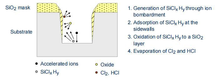
Anisotropic etch profiles are achieved by passivating the sidewalls during silicon etching. Oxygen is introduced into the etching chamber, where it reacts with the etched silicon to form silicon dioxide, which is deposited on the vertical sidewalls. Due to ion bombardment, the oxide layer on the horizontal areas is removed, allowing the lateral etching process to continue. This method can control the shape of the etch profile and the steepness of the sidewalls.
The etch rate is affected by factors such as pressure, HF generator power, process gas, actual gas flow rate and wafer temperature, and its variation range is kept below 15%. Anisotropy increases with increasing HF power, decreasing pressure and decreasing temperature. The uniformity of the etching process is determined by the gas, electrode spacing and electrode material. If the electrode distance is too small, the plasma cannot be evenly dispersed, resulting in non-uniformity. Increasing the electrode distance reduces the etching rate because the plasma is distributed in a larger volume. Carbon is the preferred electrode material because it produces a uniform strained plasma so that the edge of the wafer is affected in the same way as the center of the wafer.
The process gas plays an important role in selectivity and etching rate. For silicon and silicon compounds, fluorine and chlorine are mainly used to achieve etching. Selecting the appropriate gas, adjusting gas flow and pressure, and controlling other parameters such as temperature and power in the process can achieve the desired etch rate, selectivity, and uniformity. The optimization of these parameters is usually adjusted for different applications and materials.
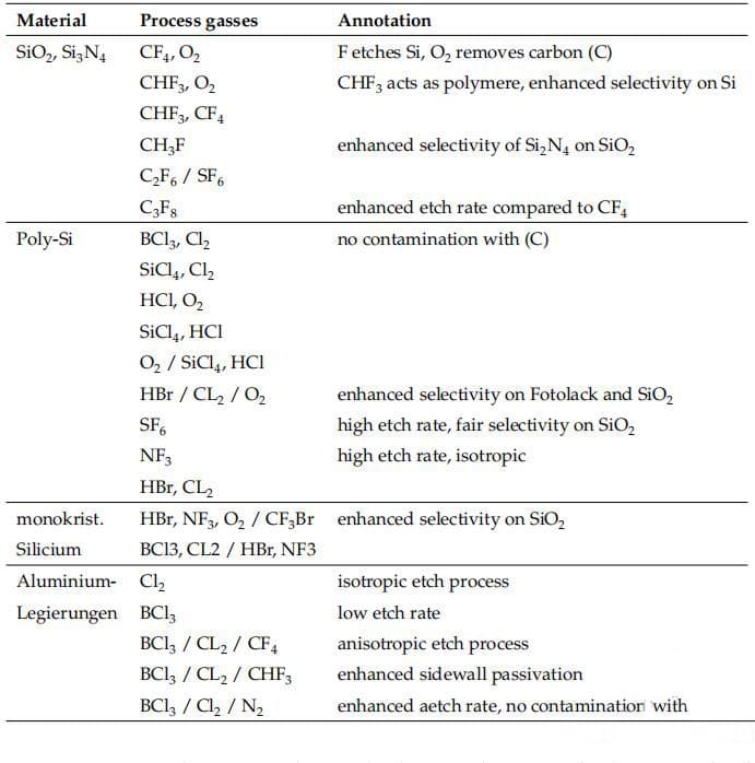
The etching process is not limited to one gas, gas mixture, or fixed process parameters. For example, the native oxide on polysilicon can be removed first with a high etch rate and low selectivity, while the polysilicon can be etched later with a higher selectivity relative to the underlying layers.
—————————————————————————————————————————————————————————————
Semicera can provide graphite parts, soft/rigid felt, silicon carbide parts,CVD silicon carbide parts,and SiC/TaC coated parts with in 30 days.
If you are interested in the above semiconductor products, please do not hesitate to contact us at the first time.
Tel: +86-13373889683
WhatsAPP:+86-15957878134
Email: sales01@semi-cera.com
Post time: Sep-12-2024