What is CVD SiC
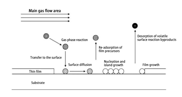
Chemical vapor deposition (CVD) is a vacuum deposition process used to produce high-purity solid materials. This process is often used in the semiconductor manufacturing field to form thin films on the surface of wafers. In the process of preparing SiC by CVD, the substrate is exposed to one or more volatile precursors, which react chemically on the surface of the substrate to deposit the desired SiC deposit. Among the many methods for preparing SiC materials, the products prepared by chemical vapor deposition have high uniformity and purity, and the method has strong process controllability.
CVD SiC materials are very suitable for use in the semiconductor industry that requires high-performance materials because of their unique combination of excellent thermal, electrical and chemical properties. CVD SiC components are widely used in etching equipment, MOCVD equipment, Si epitaxial equipment and SiC epitaxial equipment, rapid thermal processing equipment and other fields.
Overall, the largest market segment of CVD SiC components is etching equipment components. Due to its low reactivity and conductivity to chlorine- and fluorine-containing etching gases, CVD silicon carbide is an ideal material for components such as focus rings in plasma etching equipment.
CVD silicon carbide components in etching equipment include focus rings, gas shower heads, trays, edge rings, etc. Taking the focus ring as an example, the focus ring is an important component placed outside the wafer and directly in contact with the wafer. By applying voltage to the ring to focus the plasma passing through the ring, the plasma is focused on the wafer to improve the uniformity of processing.
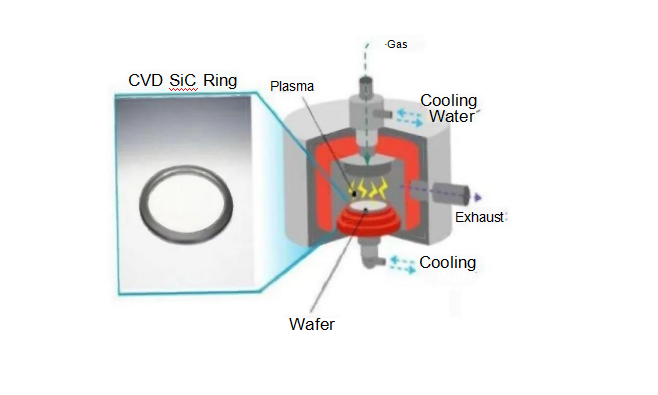
Traditional focus rings are made of silicon or quartz. With the advancement of integrated circuit miniaturization, the demand and importance of etching processes in integrated circuit manufacturing are increasing, and the power and energy of etching plasma continue to increase. In particular, the plasma energy required in capacitively coupled (CCP) plasma etching equipment is higher, so the use rate of focus rings made of silicon carbide materials is increasing. The schematic diagram of CVD silicon carbide focus ring is shown below:
Post time: Jun-20-2024