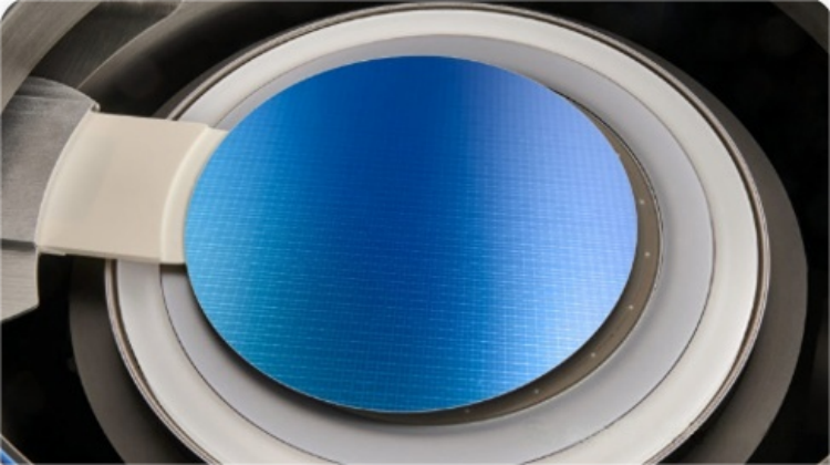
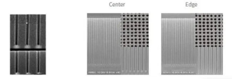
In the semiconductor manufacturing process, etching technology is a critical process that is used to precisely remove unwanted materials on the substrate to form complex circuit patterns. This article will introduce two mainstream etching technologies in detail – capacitively coupled plasma etching (CCP) and inductively coupled plasma etching (ICP), and explore their applications in etching different materials.
Capacitively coupled plasma etching (CCP)
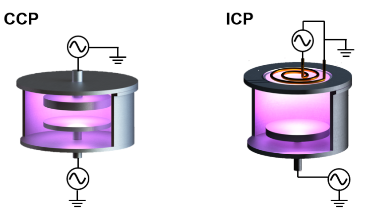
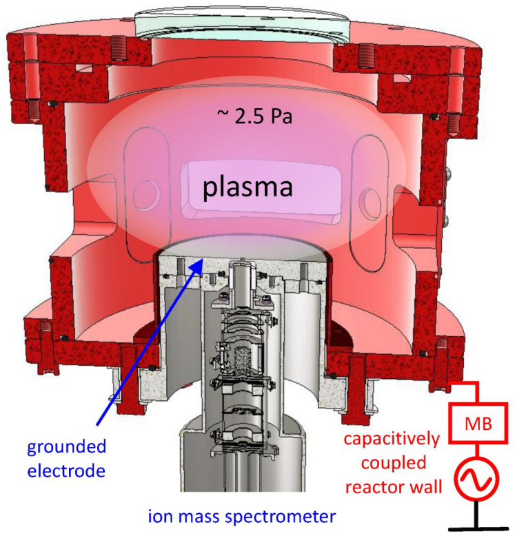
Capacitively coupled plasma etching (CCP) is achieved by applying an RF voltage to two parallel plate electrodes through a matcher and a DC blocking capacitor. The two electrodes and the plasma together form an equivalent capacitor. In this process, the RF voltage forms a capacitive sheath near the electrode, and the boundary of the sheath changes with the rapid oscillation of the voltage. When electrons reach this rapidly changing sheath, they are reflected and gain energy, which in turn triggers the dissociation or ionization of gas molecules to form plasma. CCP etching is usually applied to materials with higher chemical bond energy, such as dielectrics, but due to its lower etching rate, it is suitable for applications requiring fine control.
Inductively coupled plasma etching (ICP)
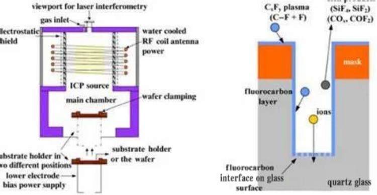
Inductively coupled plasma etching (ICP) is based on the principle that an alternating current passes through a coil to generate an induced magnetic field. Under the action of this magnetic field, the electrons in the reaction chamber are accelerated and continue to accelerate in the induced electric field, eventually colliding with the reaction gas molecules, causing the molecules to dissociate or ionize and form plasma. This method can produce a high ionization rate and allow the plasma density and bombardment energy to be adjusted independently, which makes ICP etching very suitable for etching materials with low chemical bond energy, such as silicon and metal. In addition, ICP technology also provides better uniformity and etching rate.
1. Metal etching
Metal etching is mainly used for the processing of interconnects and multi-layer metal wiring. Its requirements include: high etching rate, high selectivity (greater than 4:1 for the mask layer and greater than 20:1 for the interlayer dielectric), high etching uniformity, good critical dimension control, no plasma damage, less residual contaminants, and no corrosion to metal. Metal etching usually uses inductively coupled plasma etching equipment.
• Aluminum etching: Aluminum is the most important wire material in the middle and back stages of chip manufacturing, with the advantages of low resistance, easy deposition and etching. Aluminum etching usually uses plasma generated by chloride gas (such as Cl2). Aluminum reacts with chlorine to produce volatile aluminum chloride (AlCl3). In addition, other halides such as SiCl4, BCl3, BBr3, CCl4, CHF3, etc. can be added to remove the oxide layer on the aluminum surface to ensure the normal etching.
• Tungsten etching: In multi-layer metal wire interconnection structures, tungsten is the main metal used for the middle section interconnection of the chip. Fluorine-based or chlorine-based gases can be used to etch metal tungsten, but fluorine-based gases have poor selectivity for silicon oxide, while chlorine-based gases (such as CCl4) have better selectivity. Nitrogen is usually added to the reaction gas to obtain a high etching glue selectivity, and oxygen is added to reduce carbon deposition. Etching tungsten with chlorine-based gas can achieve anisotropic etching and high selectivity. The gases used in dry etching of tungsten are mainly SF6, Ar and O2, among which SF6 can be decomposed in plasma to provide fluorine atoms and tungsten for chemical reaction to produce fluoride.
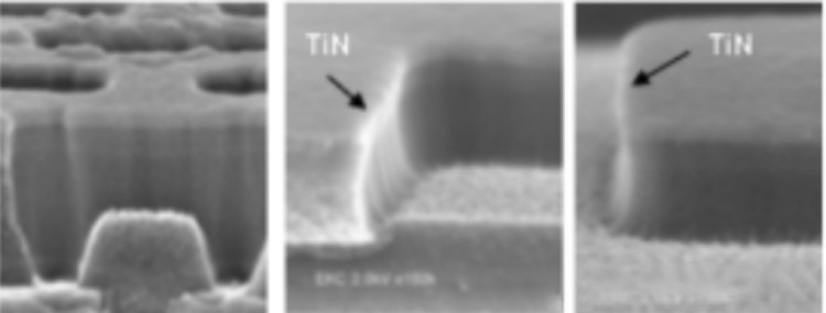
• Titanium nitride etching: Titanium nitride, as a hard mask material, replaces the traditional silicon nitride or oxide mask in the dual damascene process. Titanium nitride etching is mainly used in the hard mask opening process, and the main reaction product is TiCl4. The selectivity between the traditional mask and the low-k dielectric layer is not high, which will lead to the appearance of the arc-shaped profile on the top of the low-k dielectric layer and the expansion of the groove width after etching. The spacing between the deposited metal lines is too small, which is prone to bridge leakage or direct breakdown.
2. Insulator etching
The object of insulator etching is usually dielectric materials such as silicon dioxide or silicon nitride, which are widely used to form contact holes and channel holes to connect different circuit layers. Dielectric etching usually uses an etcher based on the principle of capacitively coupled plasma etching.
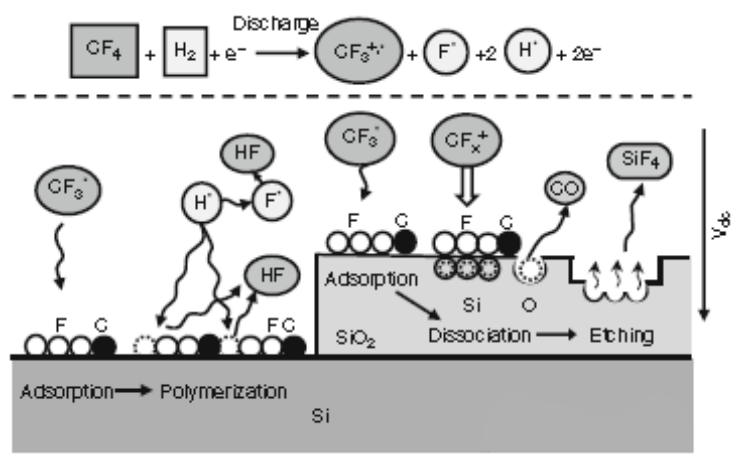
• Plasma etching of silicon dioxide film: Silicon dioxide film is usually etched using etching gases containing fluorine, such as CF4, CHF3, C2F6, SF6 and C3F8. The carbon contained in the etching gas can react with the oxygen in the oxide layer to produce byproducts CO and CO2, thereby removing the oxygen in the oxide layer. CF4 is the most commonly used etching gas. When CF4 collides with high-energy electrons, various ions, radicals, atoms and free radicals are produced. Fluorine free radicals can react chemically with SiO2 and Si to produce volatile silicon tetrafluoride (SiF4).
• Plasma etching of silicon nitride film: Silicon nitride film can be etched using plasma etching with CF4 or CF4 mixed gas (with O2, SF6 and NF3). For Si3N4 film, when CF4-O2 plasma or other gas plasma containing F atoms is used for etching, the etching rate of silicon nitride can reach 1200Å/min, and the etching selectivity can be as high as 20:1. The main product is volatile silicon tetrafluoride (SiF4) that is easy to be extracted.
3. Single crystal silicon etching
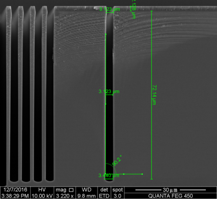
Single crystal silicon etching is mainly used to form shallow trench isolation (STI). This process usually includes a breakthrough process and a main etching process. The breakthrough process uses SiF4 and NF gas to remove the oxide layer on the surface of single crystal silicon through strong ion bombardment and the chemical action of fluorine elements; the main etching uses hydrogen bromide (HBr) as the main etchant. The bromine radicals decomposed by HBr in the plasma environment react with silicon to form volatile silicon tetrabromide (SiBr4), thereby removing silicon. Single crystal silicon etching usually uses an inductively coupled plasma etching machine.
4. Polysilicon Etching
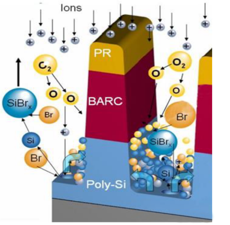
Polysilicon etching is one of the key processes that determines the gate size of transistors, and the gate size directly affects the performance of integrated circuits. Polysilicon etching requires a good selectivity ratio. Halogen gases such as chlorine (Cl2) are usually used to achieve anisotropic etching, and have a good selectivity ratio (up to 10:1). Bromine-based gases such as hydrogen bromide (HBr) can obtain a higher selectivity ratio (up to 100:1). A mixture of HBr with chlorine and oxygen can increase the etching rate. The reaction products of halogen gas and silicon are deposited on the sidewalls to play a protective role. Polysilicon etching usually uses an inductively coupled plasma etching machine.
Whether it is capacitively coupled plasma etching or inductively coupled plasma etching, each has its own unique advantages and technical characteristics. Choosing a suitable etching technology can not only improve production efficiency, but also ensure the yield of the final product.
Post time: Nov-12-2024

