The coating methods of photoresist are generally divided into spin coating, dip coating and roll coating, among which spin coating is the most commonly used. By spin coating, photoresist is dripped on the substrate, and the substrate can be rotated at high speed to obtain a photoresist film. After that, a solid film can be obtained by heating it on a hot plate. Spin coating is suitable for coating from ultra-thin films (about 20nm) to thick films of about 100um. Its characteristics are good uniformity, uniform film thickness between wafers, few defects, etc., and a film with high coating performance can be obtained.
Spin coating process
During spin coating, the main rotation speed of the substrate determines the film thickness of the photoresist. The relationship between the rotation speed and the film thickness is as follows:
Spin=kTn
In the formula, Spin is the rotation speed; T is the film thickness; k and n are constants.
Factors affecting the spin coating process
Although the film thickness is determined by the main rotation speed, it is also related to room temperature, humidity, photoresist viscosity and photoresist type. Comparison of different types of photoresist coating curves is shown in Figure 1.
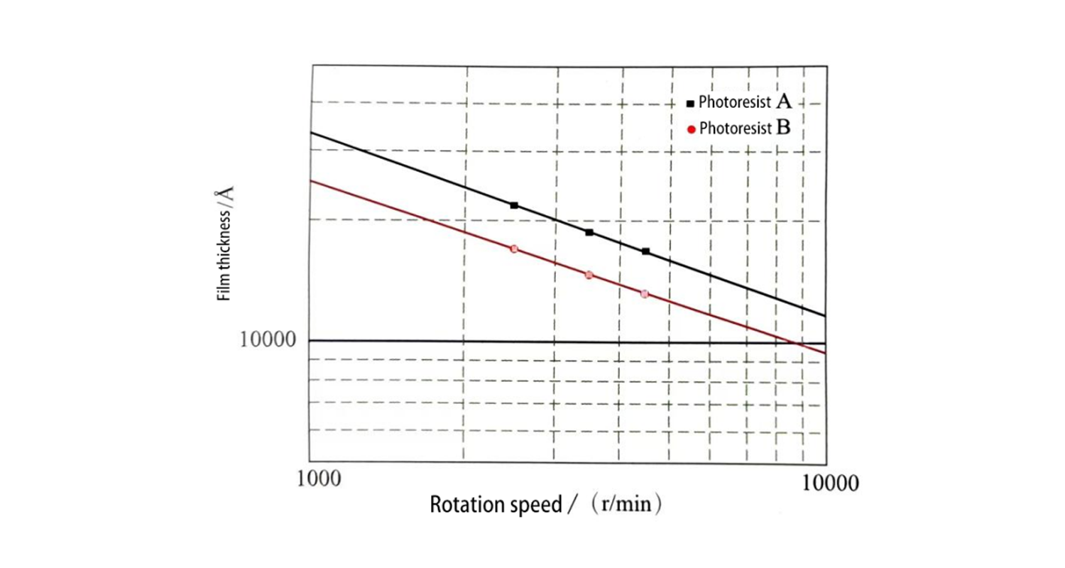
Figure 1: Comparison of different types of photoresist coating curves
The influence of main rotation time
The shorter the main rotation time, the thicker the film thickness. When the main rotation time is increased, the thinner the film becomes. When it exceeds 20s, the film thickness remains almost unchanged. Therefore, the main rotation time is usually selected to be more than 20 seconds. The relationship between the main rotation time and the film thickness is shown in Figure 2.
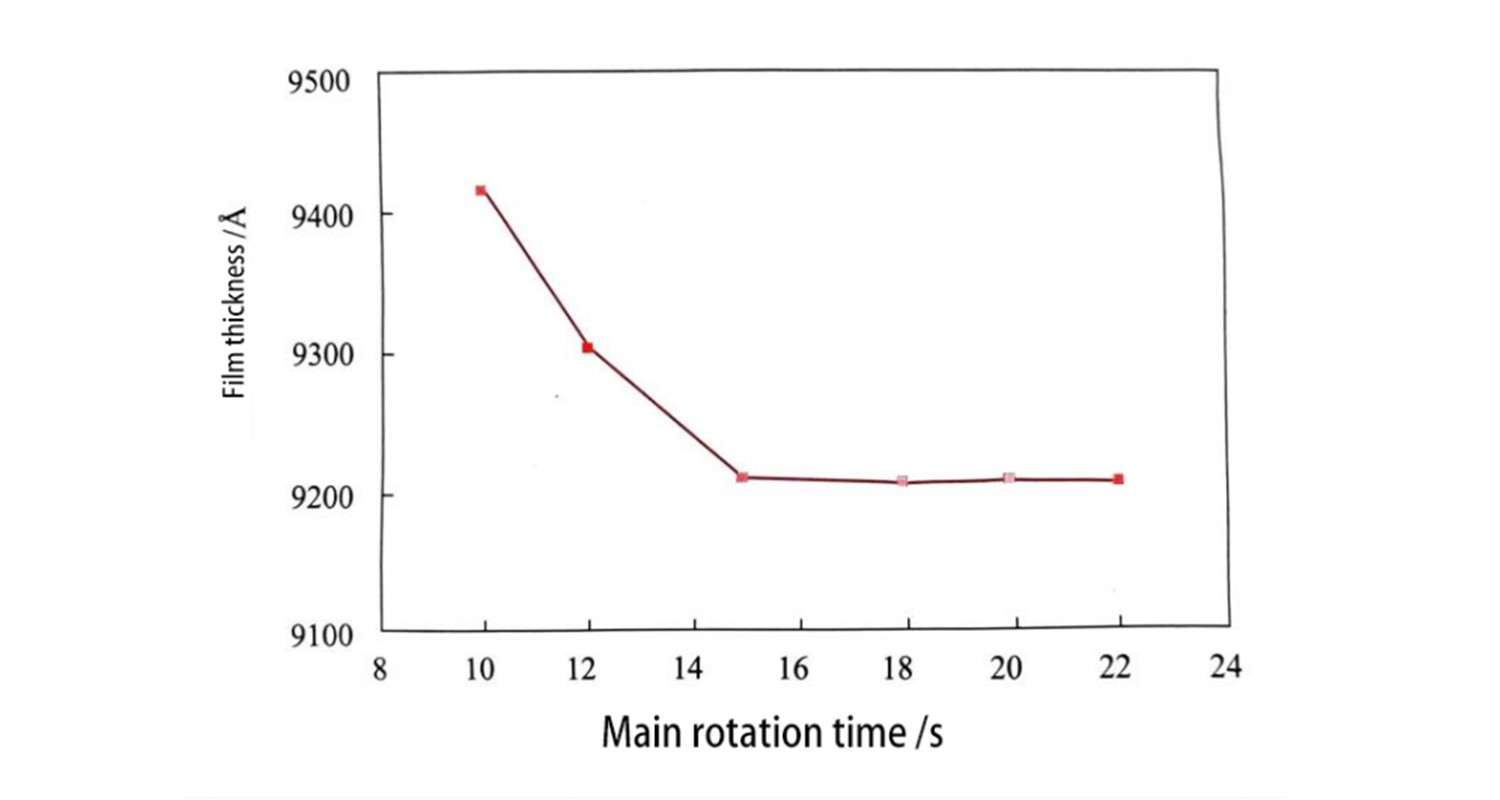
Figure 2: Relationship between main rotation time and film thickness
When the photoresist is dripped onto the substrate, even if the subsequent main rotation speed is the same, the rotation speed of the substrate during the dripping will affect the final film thickness. The thickness of the photoresist film increases with the increase of the substrate rotation speed during the dripping, which is due to the influence of solvent evaporation when the photoresist is unfolded after dripping. Figure 3 shows the relationship between the film thickness and the main rotation speed at different substrate rotation speeds during the photoresist dripping. It can be seen from the figure that with the increase of the rotation speed of the dripping substrate, the film thickness changes faster, and the difference is more obvious in the area with lower main rotation speed.
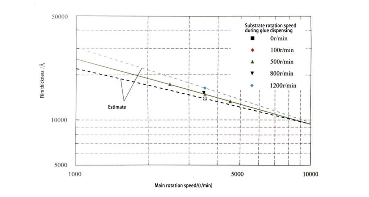
Figure 3: Relationship between film thickness and main rotation speed at different substrate rotation speeds during photoresist dispensing
Effect of humidity during coating
When humidity decreases, the film thickness increases, because the decrease in humidity promotes the evaporation of the solvent. However, the film thickness distribution does not change significantly. Figure 4 shows the relationship between humidity and film thickness distribution during coating.
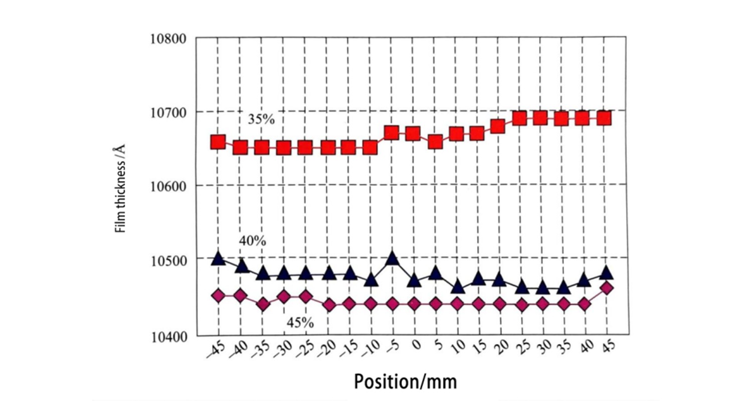
Figure 4: Relationship between humidity and film thickness distribution during coating
Effect of temperature during coating
When the indoor temperature rises, the film thickness increases. It can be seen from Figure 5 that the photoresist film thickness distribution changes from convex to concave. The curve in the figure also shows that the highest uniformity is obtained when the indoor temperature is 26°C and the photoresist temperature is 21°C.
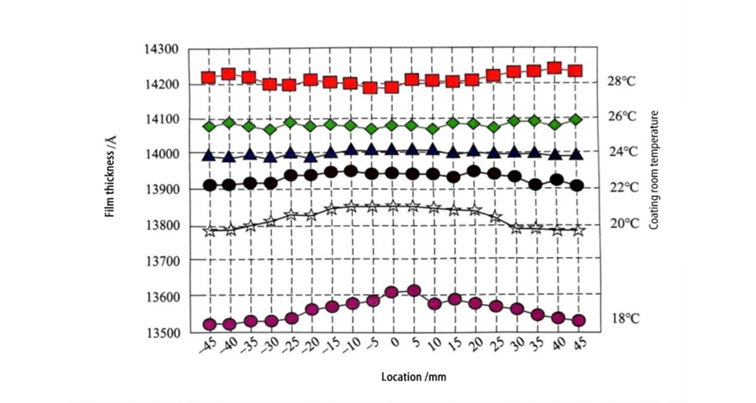
Figure 5: Relationship between temperature and film thickness distribution during coating
Effect of exhaust speed during coating
Figure 6 shows the relationship between exhaust speed and film thickness distribution. In the absence of exhaust, it shows that the center of the wafer tends to thicken. Increasing the exhaust speed will improve the uniformity, but if it is increased too much, the uniformity will decrease. It can be seen that there is an optimal value for the exhaust speed.
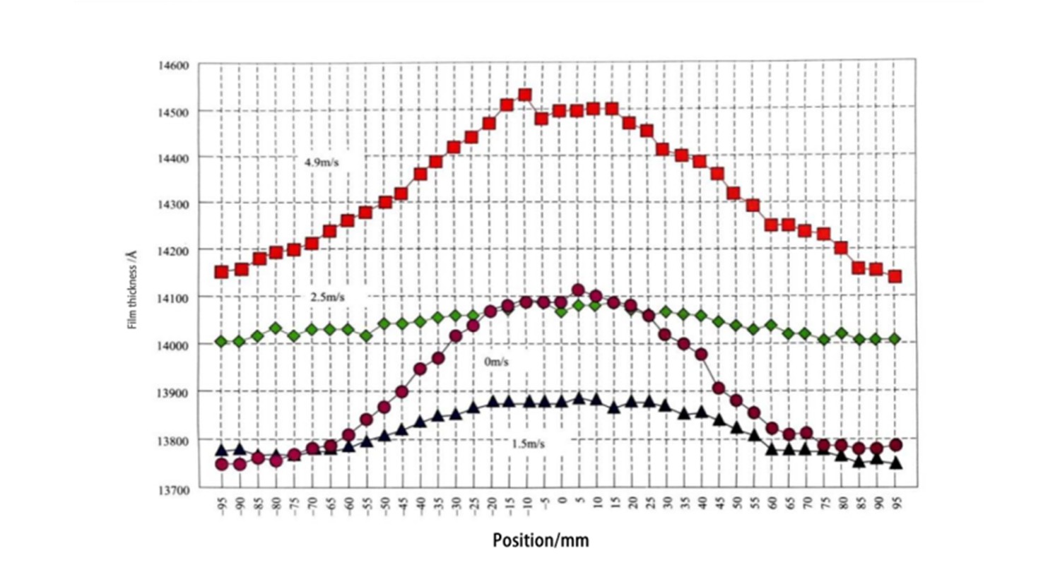
Figure 6: Relationship between exhaust speed and film thickness distribution
HMDS treatment
In order to make the photoresist more coatable, the wafer needs to be treated with hexamethyldisilazane (HMDS). Especially when moisture is attached to the surface of the Si oxide film, silanol is formed, which reduces the adhesion of the photoresist. In order to remove moisture and decompose silanol, the wafer is usually heated to 100-120°C, and mist HMDS is introduced to cause a chemical reaction. The reaction mechanism is shown in Figure 7. Through HMDS treatment, the hydrophilic surface with a small contact angle becomes a hydrophobic surface with a large contact angle. Heating the wafer can obtain higher photoresist adhesion.
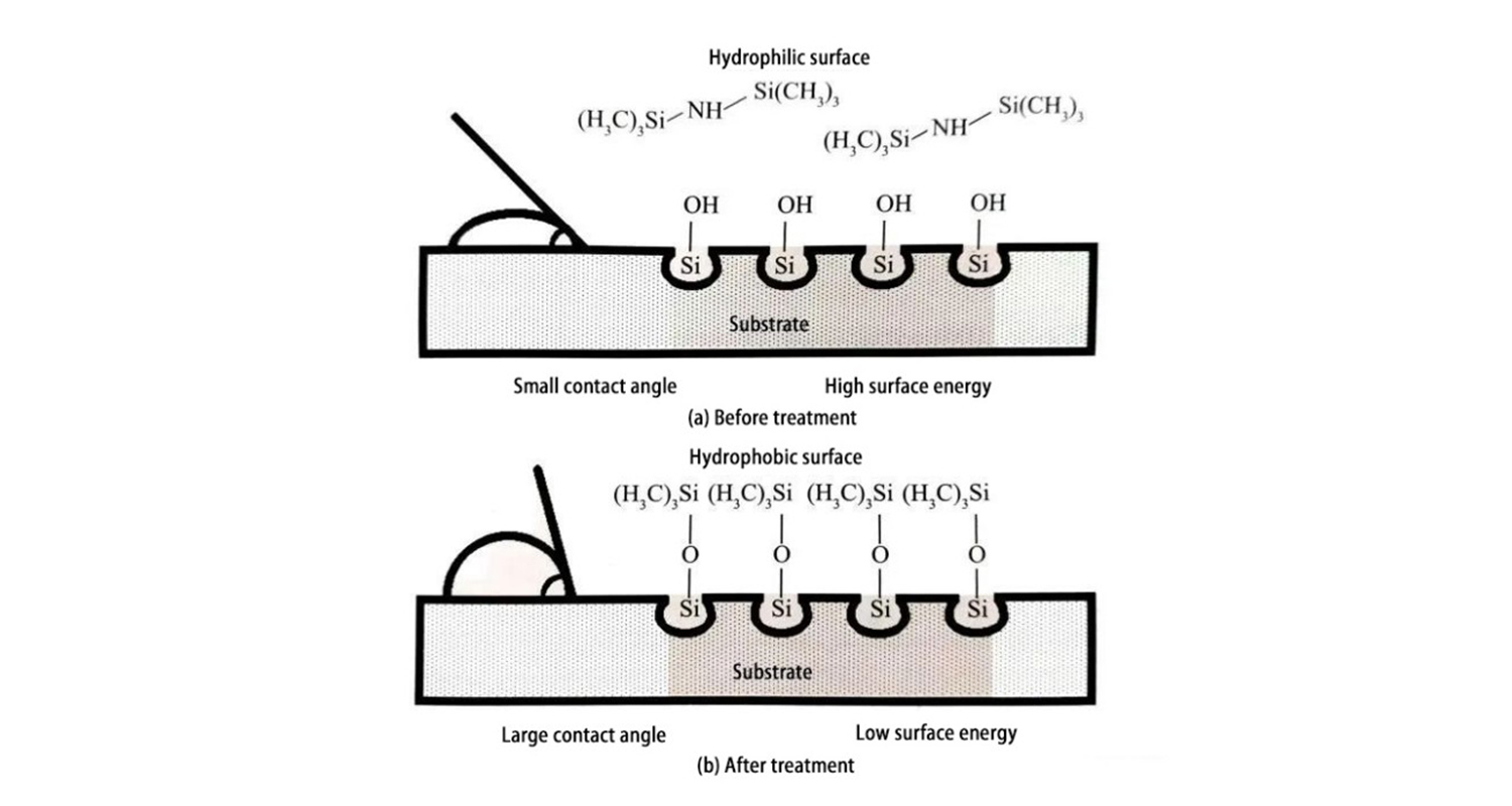
Figure 7: HMDS reaction mechanism
The effect of HMDS treatment can be observed by measuring the contact angle. Figure 8 shows the relationship between HMDS treatment time and contact angle (treatment temperature 110°C). The substrate is Si, the HMDS treatment time is greater than 1min, the contact angle is greater than 80°, and the treatment effect is stable. Figure 9 shows the relationship between HMDS treatment temperature and contact angle (treatment time 60s). When the temperature exceeds 120℃, the contact angle decreases, indicating that HMDS decomposes due to heat. Therefore, HMDS treatment is usually performed at 100-110℃.
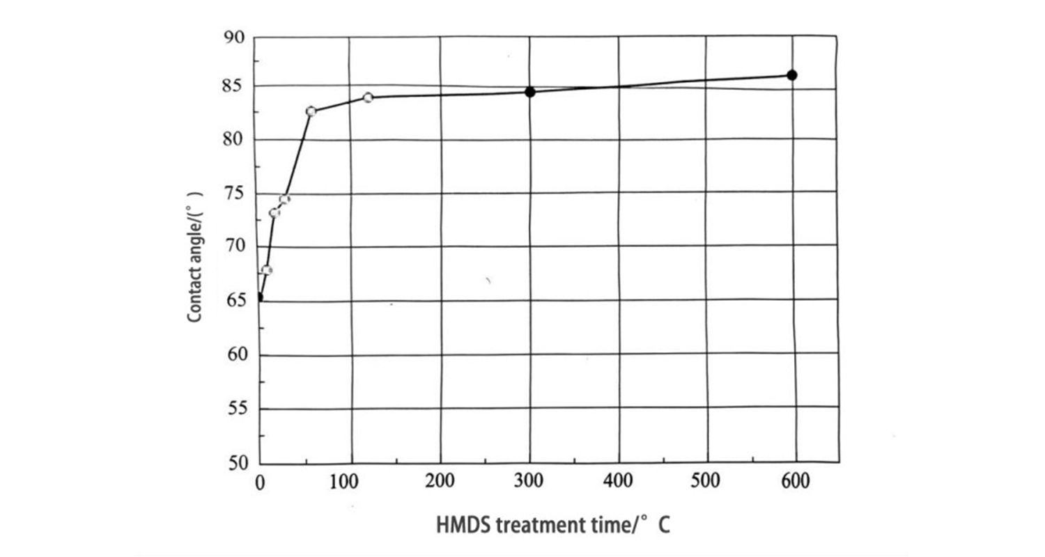
Figure 8: Relationship between HMDS treatment time
and contact angle (treatment temperature 110℃)
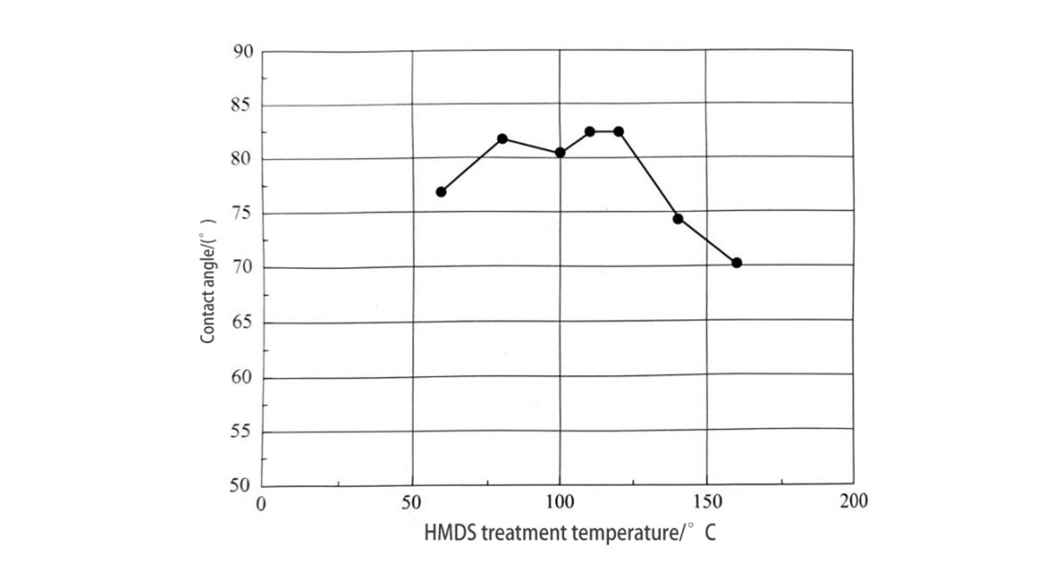
Figure 9: Relationship between HMDS treatment temperature and contact angle (treatment time 60s)
HMDS treatment is performed on a silicon substrate with an oxide film to form a photoresist pattern. The oxide film is then etched with hydrofluoric acid with a buffer added, and it is found that after HMDS treatment, the photoresist pattern can be kept from falling off. Figure 10 shows the effect of HMDS treatment (pattern size is 1um).
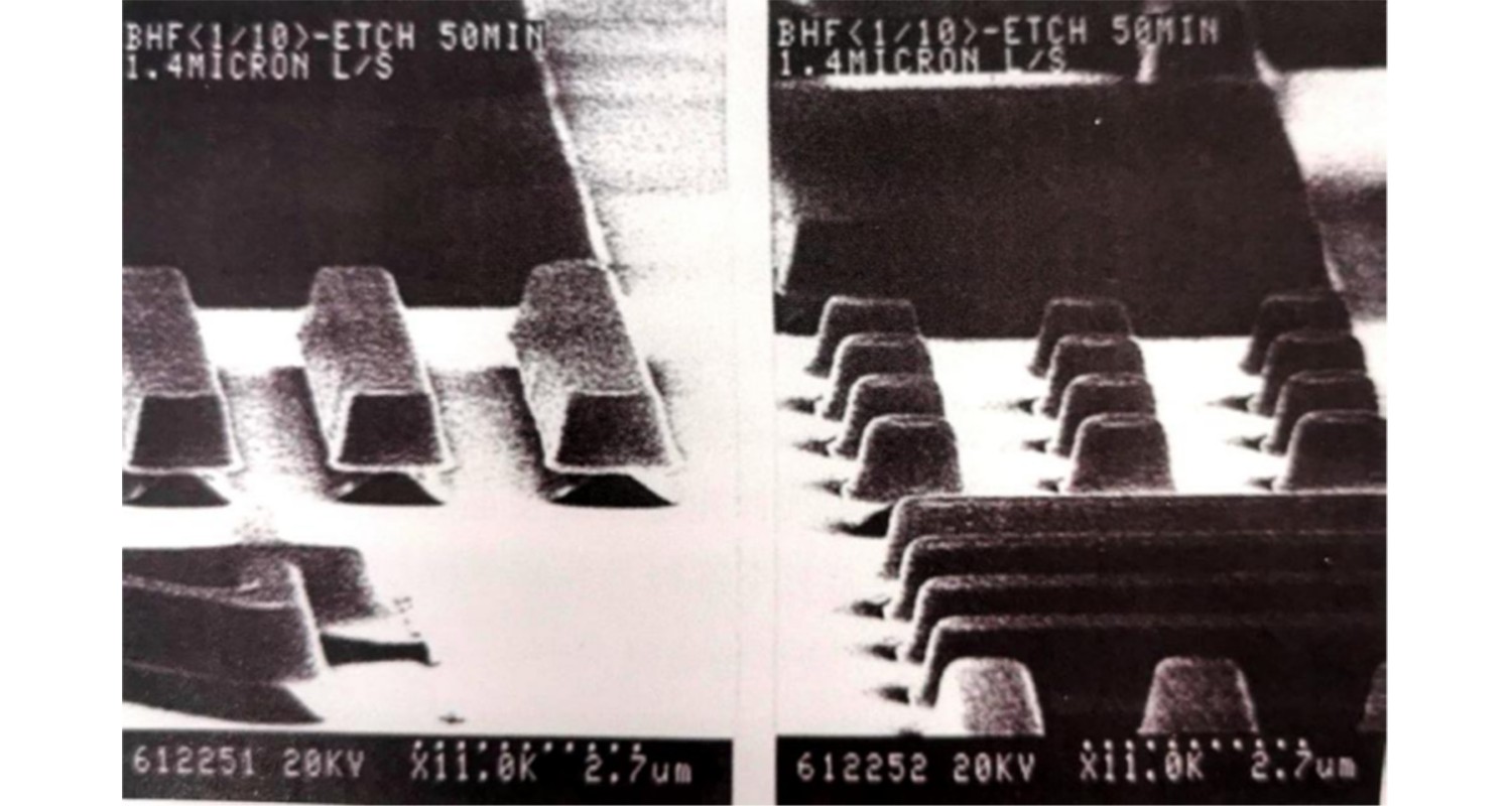
Figure 10: HMDS treatment effect (pattern size is 1um)
Prebaking
At the same rotation speed, the higher the prebaking temperature, the smaller the film thickness, which indicates that the higher the prebaking temperature, the more solvent evaporates, resulting in a thinner film thickness. Figure 11 shows the relationship between the pre-baking temperature and Dill’s A parameter. The A parameter indicates the concentration of the photosensitive agent. As can be seen from the figure, when the pre-baking temperature rises to above 140°C, the A parameter decreases, indicating that the photosensitive agent decomposes at a temperature higher than this. Figure 12 shows the spectral transmittance at different pre-baking temperatures. At 160°C and 180°C, an increase in transmittance can be observed in the wavelength range of 300-500nm. This confirms that the photosensitive agent is baked and decomposed at high temperatures. The pre-baking temperature has an optimal value, which is determined by light characteristics and sensitivity.
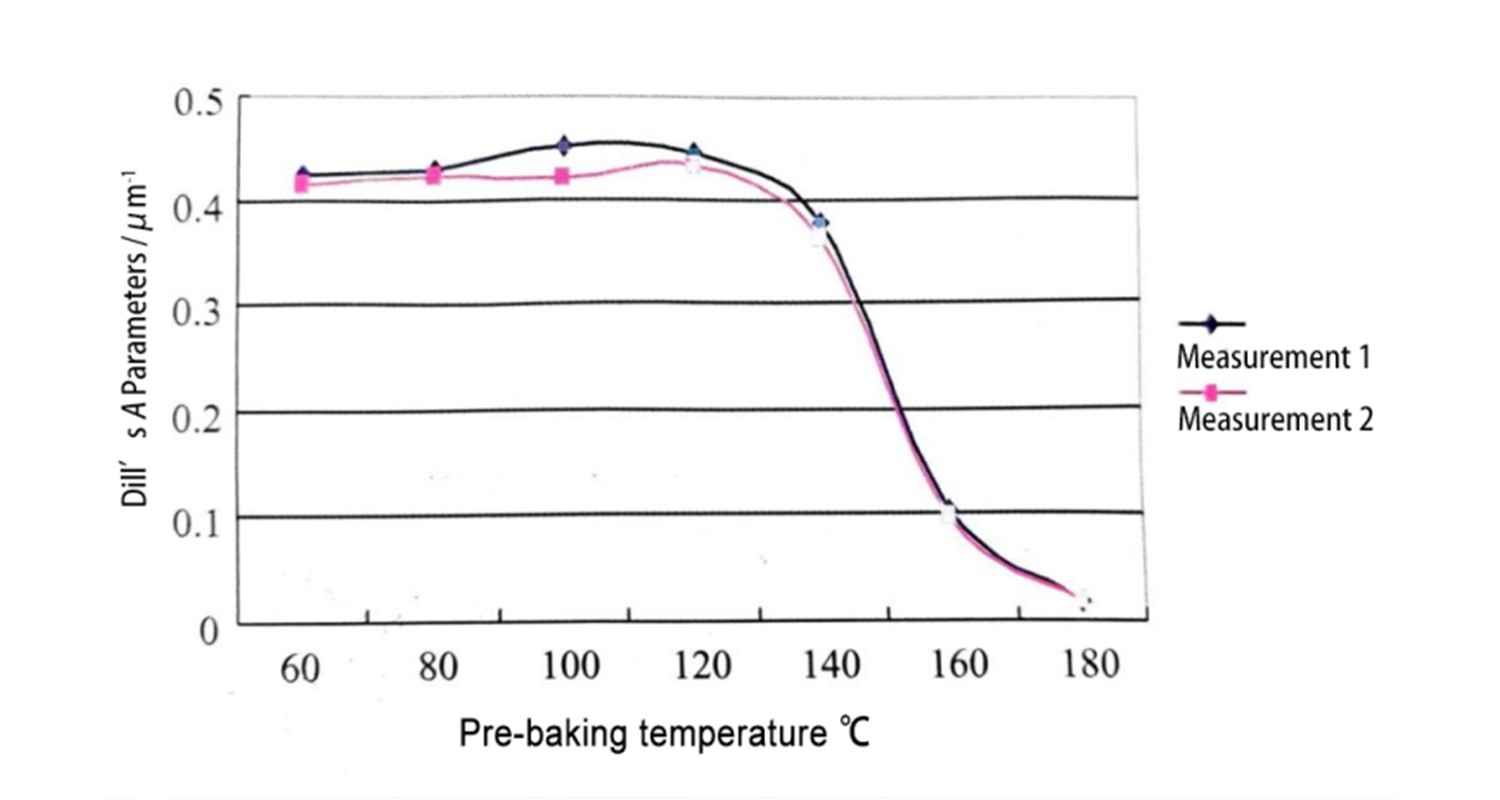
Figure 11: Relationship between pre-baking temperature and Dill’s A parameter
(measured value of OFPR-800/2)
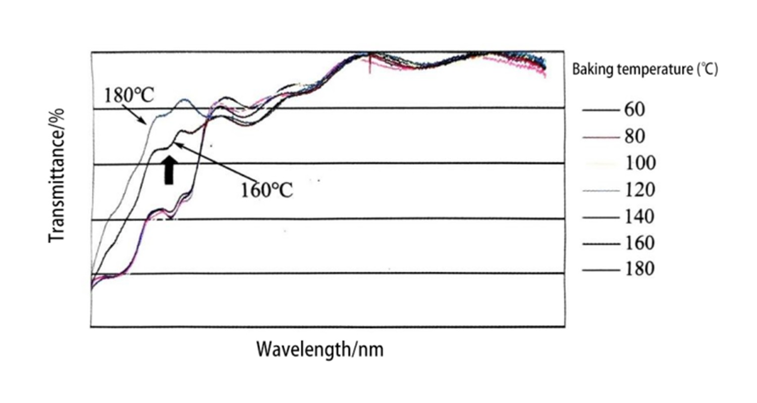
Figure 12: Spectral transmittance at different pre-baking temperatures
(OFPR-800, 1um film thickness)
In short, the spin coating method has unique advantages such as precise control of film thickness, high cost performance, mild process conditions, and simple operation, so it has significant effects in reducing pollution, saving energy, and improving cost performance. In recent years, spin coating has been gaining increasing attention, and its application has gradually spread to various fields.
Post time: Nov-27-2024