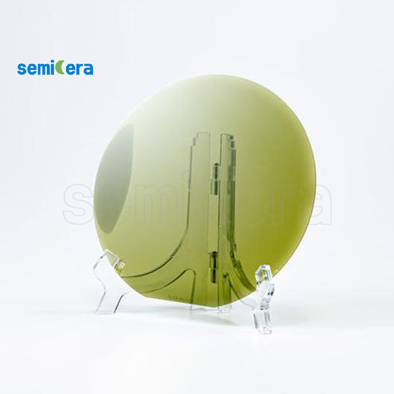
With Semicera's InP and CdTe Substrate, you can expect superior quality and precision engineered to meet the specific needs of your manufacturing processes. Whether for photovoltaic applications or semiconductor devices, our substrates are crafted to ensure optimal performance, durability, and consistency. As a trusted supplier, Semicera is committed to delivering high-quality, customizable substrate solutions that drive innovation in the electronics and renewable energy sectors.
Crystalline and Electrical Properties✽1
|
Type
|
Dopant
|
EPD(cm–2)(See below A.)
|
DF(Defect Free)area(cm2, See below B.)
|
c/(c cm–3)
|
Mobilit(y cm2/Vs)
|
Resistivit(y Ω・cm)
|
|
n
|
Sn
|
≦5×10⁴
≦1×10⁴
≦5×10³
|
──────
|
(0.5〜6)×1018
|
──────
|
──────
|
|
n
|
S
|
──────
|
≧ 10(59.4%)
≧ 15(87%).4
|
(2〜10)×1018
|
──────
|
──────
|
| p |
Zn
|
──────
|
≧ 10(59.4%)
≧ 15(87%).
|
(3〜6)×1018
|
──────
|
──────
|
|
S.I.
|
Fe
|
≦5×10⁴
≦1×10⁴
|
──────
|
──────
|
──────
|
≧ 1×10⁶
|
|
n
|
none
|
≦5×10⁴
|
──────
|
≦1×10¹⁶
|
≧ 4×10³
|
──────
|
✽1 Other specifications are available upon request.
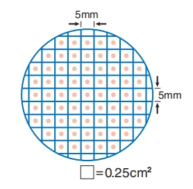
A.13 Points Average
1. Dislocation etch pit densities are measured at 13 points.
2. Area weighted average of the dislocation densities is calculated.
B.DF Area Measurement (In Case of Area Guarantee)
1. Dislocation etch pit densities of 69 points shown as right are counted.
2. DF is defined as EPD less than 500cm–2
3. Maximum DF area measured by this method is 17.25cm2
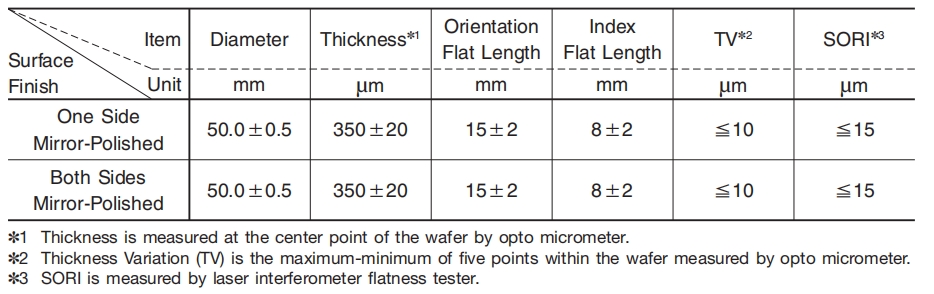
InP Single Crystal Substrates Common Specifications
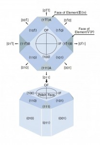
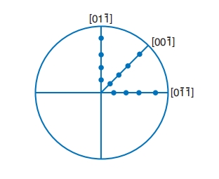
1. Orientation
Surface orientation (100)±0.2º or (100)±0.05º
Surface off orientation is available upon request.
Orientation of flat OF : (011)±1º or (011)±0.1º IF : (011)±2º
Cleaved OF is available upon request.
2. Laser marking based on SEMI standard is available.
3. Individual package,as well as package in N2 gas are available.
4. Etch-and-pack in N2 gas is available.
5. Rectangular wafers are available.
Above specification is of JX' standard.
If other specifications are required, please inquire us.
Orientation