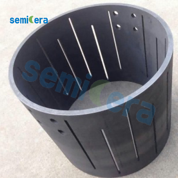
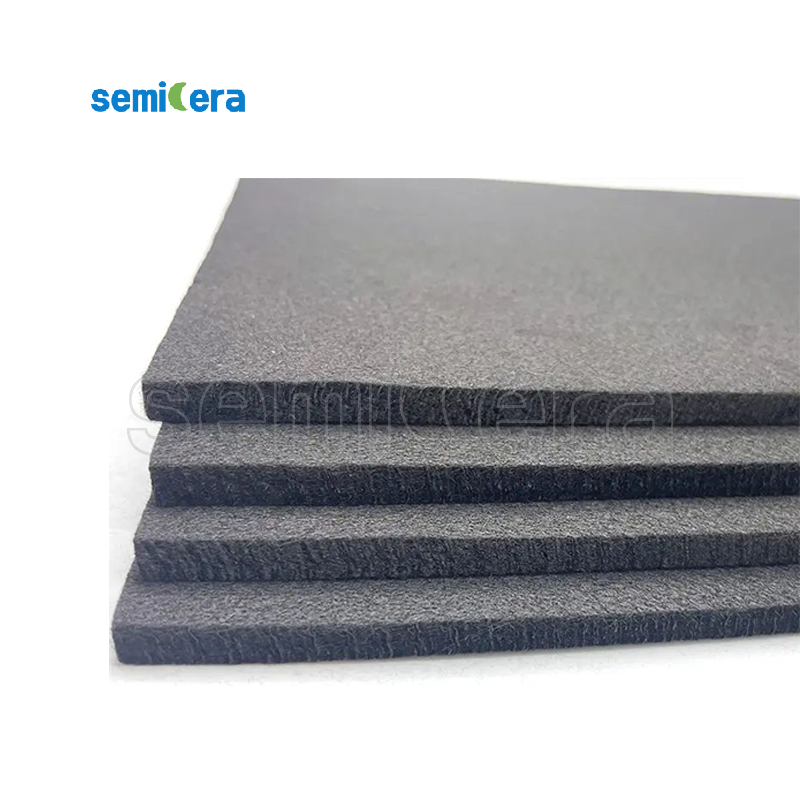
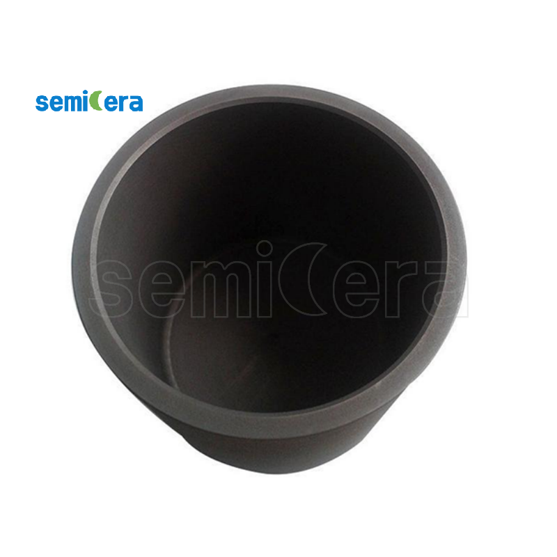
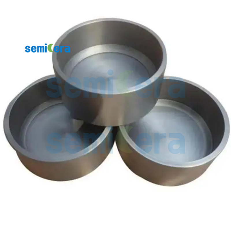
Introducing Atomic Layer Deposition, a cutting-edge technology revolutionizing the semiconductor industry. Developed by Semicera Semiconductor Technology Co., Ltd., a leading manufacturer and supplier in China, this advanced process offers unparalleled precision and control in depositing thin film materials onto semiconductor substrates. Using a unique layer-by-layer approach, Atomic Layer Deposition enables the production of high-performance, low-defect semiconductor devices with enhanced electrical and optical properties. This innovative technology is ideal for manufacturing a wide range of semiconductor products, including integrated circuits, solar cells, and nanoelectronics. As a trusted factory in the semiconductor industry, Semicera Semiconductor Technology Co., Ltd. is committed to providing top-quality Atomic Layer Deposition equipment and services that meet the diverse needs of its global customers. With its expertise and state-of-the-art facilities, the company has earned a reputation for delivering reliable and cost-effective solutions to drive technological advancements in the semiconductor field. Experience the future of semiconductor manufacturing with Atomic Layer Deposition from Semicera Semiconductor Technology Co., Ltd.