Semicera 3C-SiC Wafer Substrates are engineered to provide a robust platform for next-generation power electronics and high-frequency devices. With superior thermal properties and electrical characteristics, these substrates are designed to meet the demanding requirements of modern technology.
The 3C-SiC (Cubic Silicon Carbide) structure of Semicera Wafer Substrates offers unique advantages, including higher thermal conductivity and a lower thermal expansion coefficient compared to other semiconductor materials. This makes them an excellent choice for devices operating under extreme temperatures and high-power conditions.
With a high electrical breakdown voltage and superior chemical stability, Semicera 3C-SiC Wafer Substrates ensure long-lasting performance and reliability. These properties are critical for applications such as high-frequency radar, solid-state lighting, and power inverters, where efficiency and durability are paramount.
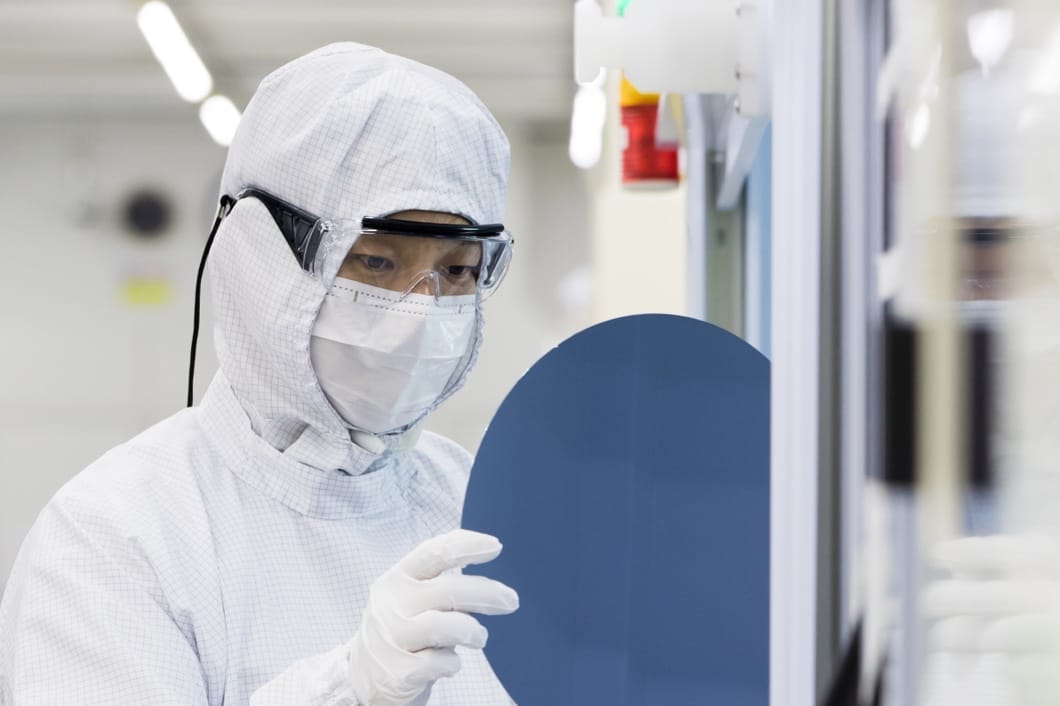
Semicera's commitment to quality is reflected in the meticulous manufacturing process of their 3C-SiC Wafer Substrates, ensuring uniformity and consistency across every batch. This precision contributes to the overall performance and longevity of the electronic devices built upon them.
By choosing Semicera 3C-SiC Wafer Substrates, manufacturers gain access to a cutting-edge material that enables the development of smaller, faster, and more efficient electronic components. Semicera continues to support technological innovation by providing reliable solutions that meet the evolving demands of the semiconductor industry.
|
Items |
Production |
Research |
Dummy |
|
Crystal Parameters |
|||
|
Polytype |
4H |
||
|
Surface orientation error |
<11-20 >4±0.15° |
||
|
Electrical Parameters |
|||
|
Dopant |
n-type Nitrogen |
||
|
Resistivity |
0.015-0.025ohm·cm |
||
|
Mechanical Parameters |
|||
|
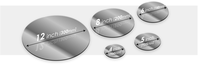
Diameter |
150.0±0.2mm |
||
|
Thickness |
350±25 μm |
||
|
Primary flat orientation |
[1-100]±5° |
||
|
Primary flat length |
47.5±1.5mm |
||
|
Secondary flat |
None |
||
|
TTV |
≤5 μm |
≤10 μm |
≤15 μm |
|
LTV |
≤3 μm(5mm*5mm) |
≤5 μm(5mm*5mm) |
≤10 μm(5mm*5mm) |
|
Bow |
-15μm ~ 15μm |
-35μm ~ 35μm |
-45μm ~ 45μm |
|
Warp |
≤35 μm |
≤45 μm |
≤55 μm |
|
Front(Si-face) roughness(AFM) |
Ra≤0.2nm (5μm*5μm) |
||
|
Structure |
|||
|
Micropipe density |
<1 ea/cm2 |
<10 ea/cm2 |
<15 ea/cm2 |
|
Metal impurities |
≤5E10atoms/cm2 |
NA |
|
|
BPD |
≤1500 ea/cm2 |
≤3000 ea/cm2 |
NA |
|
TSD |
≤500 ea/cm2 |
≤1000 ea/cm2 |
NA |
|
Front Quality |
|||
|
Front |
Si |
||
|
Surface finish |
Si-face CMP |
||
|
Particles |
≤60ea/wafer (size≥0.3μm) |
NA |
|
|
Scratches |
≤5ea/mm. Cumulative length ≤Diameter |
Cumulative length≤2*Diameter |
NA |
|
Orange peel/pits/stains/striations/ cracks/contamination |
None |
NA |
|
|
Edge chips/indents/fracture/hex plates |
None |
||
|
Polytype areas |
None |
Cumulative area≤20% |
Cumulative area≤30% |
|
Front laser marking |
None |
||
|
Back Quality |
|||
|
Back finish |
C-face CMP |
||
|
Scratches |
≤5ea/mm,Cumulative length≤2*Diameter |
NA |
|
|
Back defects (edge chips/indents) |
None |
||
|
Back roughness |
Ra≤0.2nm (5μm*5μm) |
||
|
Back laser marking |
1 mm (from top edge) |
||
|
Edge |
|||
|
Edge |
Chamfer |
||
|
Packaging |
|||
|
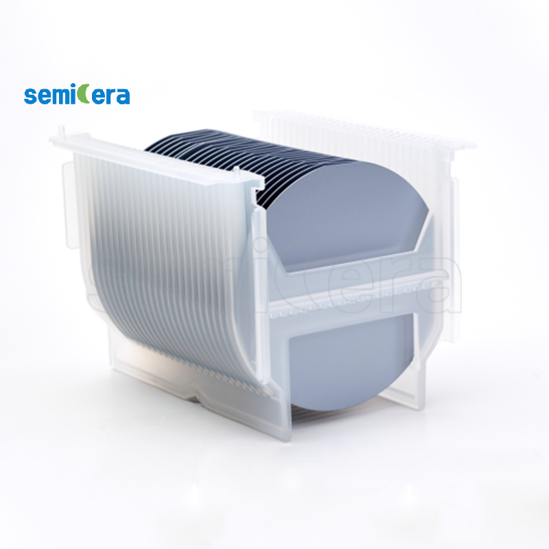
Packaging |
Epi-ready with vacuum packaging Multi-wafer cassette packaging |
||
|
*Notes: "NA" means no request Items not mentioned may refer to SEMI-STD. |
|||