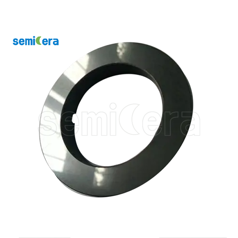
Semicera’s 2~6 inch 4° off-angle P-type 4H-SiC substrates are engineered to meet the growing needs of high-performance power and RF device manufacturers. The 4° off-angle orientation ensures optimized epitaxial growth, making this substrate an ideal foundation for a range of semiconductor devices, including MOSFETs, IGBTs, and diodes.
This 2~6 inch 4° off-angle P-type 4H-SiC substrate has excellent material properties, including high thermal conductivity, excellent electrical performance, and outstanding mechanical stability. The off-angle orientation helps reduce micropipe density and promotes smoother epitaxial layers, which is critical to improving the performance and reliability of the final semiconductor device.
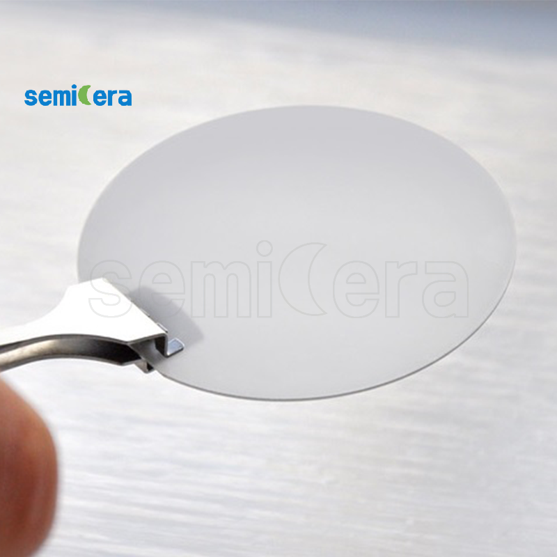
Semicera’s 2~6 inch 4° off-angle P-type 4H-SiC substrates are available in a variety of diameters, ranging from 2 inches to 6 inches, to meet different manufacturing requirements. Our substrates are precisely engineered to provide uniform doping levels and high-quality surface characteristics, ensuring that each wafer meets the stringent specifications required for advanced electronic applications.
Semicera's commitment to innovation and quality ensures that our 2~6 inch 4° off-angle P-type 4H-SiC substrates deliver consistent performance in a wide range of applications from power electronics to high-frequency devices. This product provides a reliable solution for the next generation of energy-efficient, high-performance semiconductors, supporting technological advancements in industries such as automotive, telecommunications, and renewable energy.
Size-related standards
|
Size |
2-Inch |
4-Inch |
| Diameter | 50.8 mm±0.38 mm | 100.0 mm+0/-0.5 mm |
| Surface Orentation | 4°toward<11-20>±0.5° | 4°toward<11-20>±0.5° |
| Primary Flat Length | 16.0 mm±1.5mm | 32.5mm±2mm |
| Secondary Flat Length | 8.0 mm±1.5mm | 18.0 mm ± 2 mm |
| Primary Flat Orientation | Parallelto <11-20>±5.0° | Parallelto<11-20>±5.0c |
| Secondary Flat Orientation | 90°CW from primary ± 5.0°,silicon face up | 90°CW from primary ± 5.0°,silicon face up |
| Surface Finish | C-Face: Optical Polish, Si-Face: CMP | C-Face:OpticalPolish, Si-Face: CMP |
| Wafer Edge | Beveling | Beveling |
| Surface Roughness | Si-Face Ra<0.2 nm | Si-Face Ra<0.2nm |
| Thickness | 350.0±25.0um | 350.0±25.0um |
| Polytype | 4H | 4H |
| Doping | p-Type | p-Type |
Size-related standards
|
Size |
6-Inch |
| Diameter | 150.0 mm+0/-0.2 mm |
| Surface Orientation | 4°toward<11-20>±0.5° |
| Primary Flat Length | 47.5 mm ± 1.5mm |
| Secondary Flat Length | None |
| Primary Flat Orientation | Parallel to <11-20>±5.0° |
| SecondaryFlat Orientation | 90°CW from primary ± 5.0°, silicon face up |
| Surface Finish | C-Face: Optical Polish, Si-Face:CMP |
| Wafer Edge | Beveling |
| Surface Roughness | Si-Face Ra<0.2 nm |
| Thickness | 350.0±25.0μm |
| Polytype | 4H |
| Doping | p-Type |
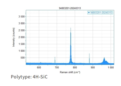
Raman
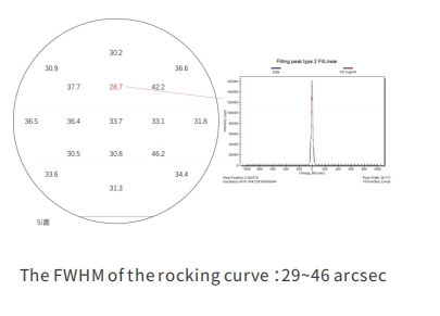
Rocking curve
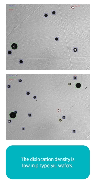
Dislocation density (KOH etching)
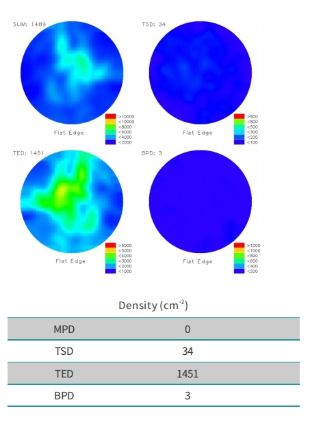
KOH etching images